Virtex-4 FPGA Configuration User Guide www.xilinx.com 81
UG071 (v1.12) June 2, 2017
Dynamic Reconfiguration of Functional Blocks (DRP)
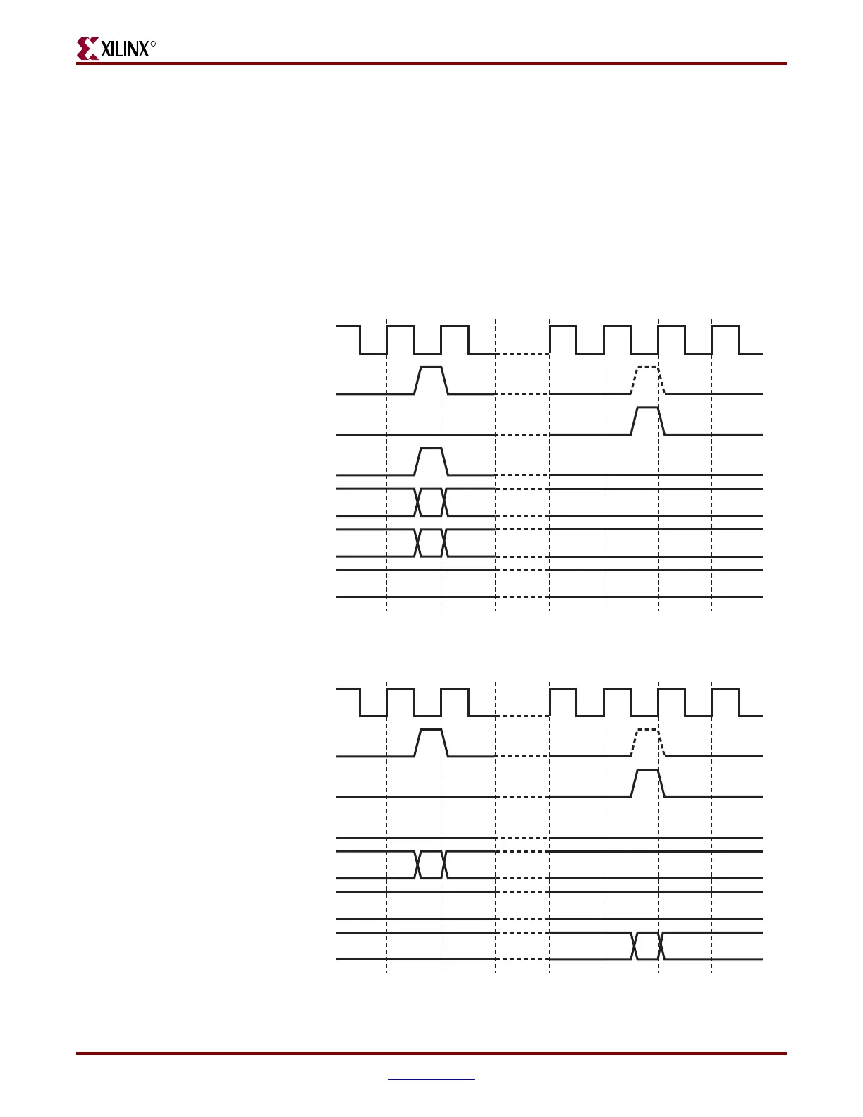
Synchronous timing for the port is provided by the DCLK input, and all the other input
signals are registered in the functional block on the rising edge of DCLK. Input (write) data
is presented simultaneously with the write address and DWE and DEN signals prior to the
next positive edge of DCLK. The port asserts DRDY for one clock cycle when it is ready to
accept more data. The timing requirements relative to DCLK for all the other signals are the
same. The output data is not registered in the functional blocks. Output (read) data is
available after some cycles following the cycle that DEN and DADDR are asserted. The
availability of output data is indicated by the assertion of DRDY.
Figure 6-4 and Figure 6-5 show the timing relationships between the port signals for write
and read operations. Absolute timing parameters, such as maximum DCLK frequency,
setup time, etc., are defined in the Virtex-4 FPGA Data Sheet.
Figure 6-4: Write Timing with Wait States
Figure 6-5: Read Timing with Wait States
bb
BB
DCLK
DEN
DRDY
DWE
DADDR[m:0]
DI[n:0]
DO[n:0]
ds071_44_123003
aa
AA
DCLK
DEN
DRDY
DWE
DADDR[m:0]
DI[n:0]
DO[n:0]
ds071_45_031804

 Loading...


