28 www.xilinx.com Virtex-4 FPGA Configuration User Guide
UG071 (v1.12) June 2, 2017
Chapter 2: Configuration Interfaces
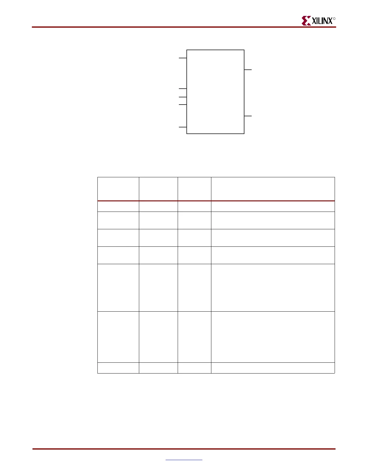
Table 2-2 describes the Serial Configuration Interface.
Figure 2-1: Virtex-4 Serial Configuration Interface
Table 2-2: Virtex-4 Serial Configuration Interface Pins
Pin Name Type
Dedicated
or Dual-
Purpose
Description
M[2:0] Input Dedicated Mode Pins – determine configuration mode.
CCLK
Input or
Output
Dedicated
Configuration clock source for all configuration
modes except JTAG.
D_IN Input Dedicated
Serial configuration data input, synchronous to
rising CCLK edge.
DOUT_BUSY Output Dedicated
Serial data output for downstream daisy-chained
devices.
DONE
Bidirectional,
open-drain
or active
Dedicated
Active High signal indicating configuration is
complete:
0 = FPGA not configured
1 = FPGA configured
Refer to the “BitGen” section of the Development
System Reference Guide for software settings.
INIT_B
Input or
Output,
open-drain
Dedicated
Before the MODE pins are sampled, INIT_B is an
input that can be held Low to delay configuration.
After the MODE pins are sampled, INIT_B is an
open-drain active Low output indicating whether
a CRC error occurred during configuration:
0 = CRC error
1 = No CRC error
PROGRAM_B Input Dedicated Active-Low asynchronous full-chip reset.
DOUT
DONE
CCLK
PROGRAM_B
INIT_B
D_IN
M[2:0]
ug071_14_073007

 Loading...


