58 www.xilinx.com Virtex-4 FPGA Configuration User Guide
UG071 (v1.12) June 2, 2017
Chapter 3: Boundary-Scan and JTAG Configuration
For JTAG configuration mode, JTAG inputs use the V
CCO_CFG
supply.
Table 3-1: Virtex-4 TAP Controller Pins
Pin Description
TDI Test Data In. This pin is the serial input to all JTAG instruction and data registers.
The state of the TAP controller and the current instruction determine the register that
is fed by the TDI pin for a specific operation. TDI has an internal resistive pull-up to
provide a logic High to the system if the pin is not driven. TDI is applied into the JTAG
registers on the rising edge of TCK.
TDO Test Data Out. This pin is the serial output for all JTAG instruction and data registers.
The state of the TAP controller and the current instruction determine the register
(instruction or data) that feeds TDO for a specific operation. TDO changes state on the
falling edge of TCK and is only active during the shifting of instructions or data
through the device. TDO is an active driver output.
TMS Test Mode Select. This pin determines the sequence of states through the TAP
controller on the rising edge of TCK.
TMS has an internal resistive pull-up to provide a logic High if the pin is not driven.
TCK Test Clock. This pin is the JTAG Test Clock.
TCK sequences the TAP controller and the JTAG registers in the Virtex-4 devices.
Notes:
1. As specified by the IEEE Standard, the TMS and TDI pins both have internal pull-up resistors. These
internal pull-up resistors of 50-150 kΩ are active, regardless of the mode selected.
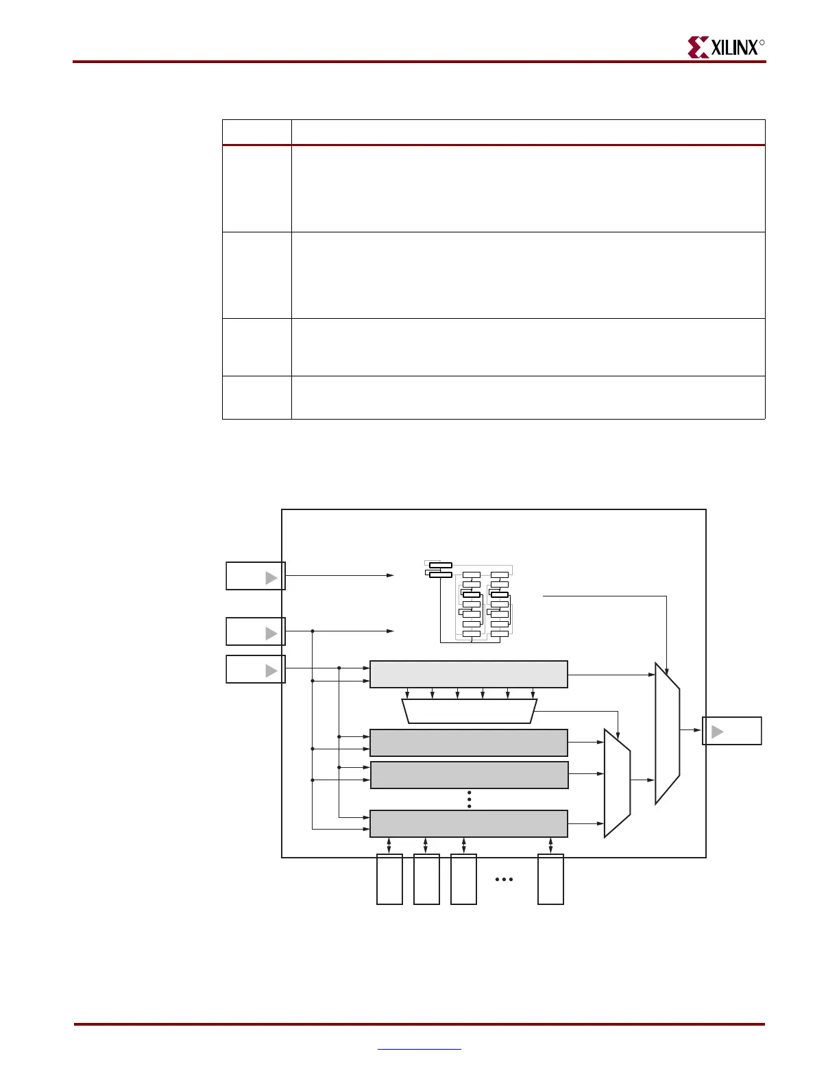
Figure 3-1: Typical JTAG Architecture
IEEE Standard 1149.1 Compliant Device
TMS
Instruction Register
Instruction Decoder
Bypass[1] Register
IDCODE[32] Register
Boundary-Scan[N] Register
Select Data
Register
Shift-IR/Shift-DR
Select Next State
TAP State Machine
TCK
TDI
TDO
I/O I/O I/O I/O
Test-Logic-Reset
Run-Test/Idle
Select-DR
Capture-DR
Shift-DR
Exit1-DR
Pause-DR
Exit2-DR
Update-DR
0
0
0
0
0
0
0
0
1
1
1
1
1
1
1
Select-IR
Capture-IR
Shift-IR
Exit1-IR
Pause-IR
Exit2-IR
Update-IR
0
0
0
0
0
0
1
1
1
1
1
1
0
0
11
UG071_47_042704

 Loading...


