UG-1828 Preliminary Technical Data
Rev. PrB | Page 116 of 277
tracking calibrations including DPD operations in such a system. However, in a 1Tx1Rx FDD system, because one receiver is always idle,
it can be used as an observation channel. For example, if Transmitter 1 is transmitting, then Receiver 1 can be used for observation by
receiving loop back signals from Transmitter 1 and Receiver 2 can be used as the main receive path. Note it is required that the
observation must be at the same side of the transmitter it observes so observation channel 1 is always for Transmitter 1 and observation
channel 2 is always for Transmitter 2. When users are in control of the observation channel, they will be allowed to configure the ORx
based on their requirements such as the ORx gain. When the ADRV9001 device is control of the observation channel, it is responsible to
configure the observation channel properly without any user intervention.
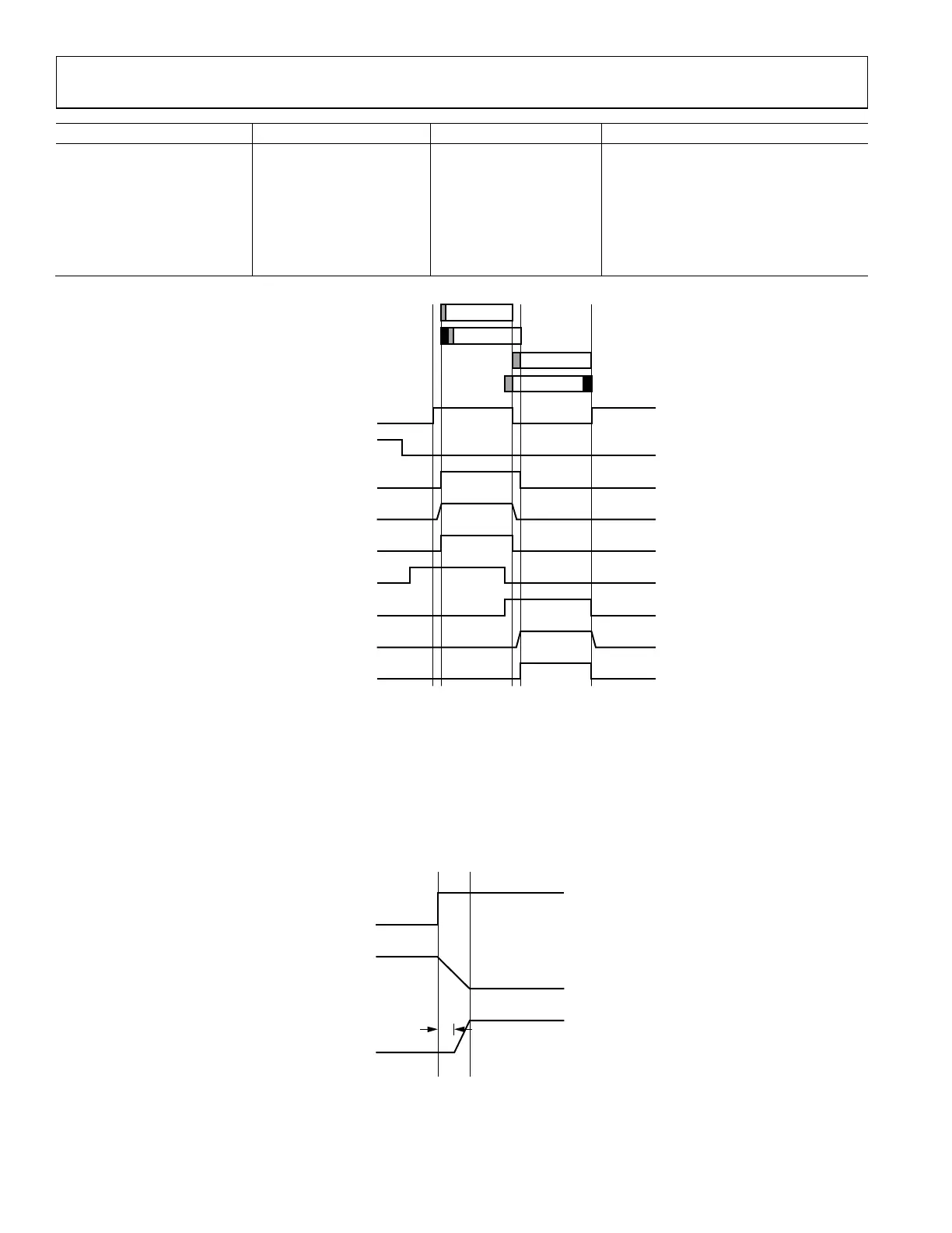
As shown in Figure 123, each receiver has 3 inputs, one is the ILB input dedicated for receiving ILB signal. The others are Rx1A/Rx2A
and Rx1B/Rx2B inputs, one could be configured to receive RF signals and the other one to receive ELB signals.
Due to the support of a wide range of applications, user interaction with the receiver signal chain is mainly done through configuration
profiles. Based on the channel profile, which includes key parameters such as bandwidth, sample rate and AGC settings, initial
calibration is performed in the device to set up the receive chain properly. When DPD is performed internally in the device, the switch
between receiver and ORx is fully determined without user interaction. Therefore, the device could support rapid switching between
different RF channel profiles with different modulation schemes and bandwidths requirements. When DPD is performed externally by
baseband processor, then baseband processor owns the entire ORx channel. It is the user’s responsibility to make sure there is no conflict
between the DPD operations and the transmitter tracking calibrations in the device.
In the ADRV9001, a specialized “Monitor mode” exists that allows the device to autonomously poll a region of the spectrum for the
presence of a signal, while in a low power state. In this mode, the chip continuously cycles through sleep-detect-sleep states controlled by
an internal state machine. Power savings are achieved by ensuring that the sleep duty cycle is greater than the “detect” duty cycle. In the
“sleep” state, the chip is in a minimal power consumption configuration where few functions are enabled. After a pre-determined period,
the chip enters the “detect” state. In this state, the chip enables a receiver and performs a signal detect over a bandwidth and at a receiver
LO frequency determined by the user. If a signal is detected, the “Monitor Mode” state machine exits its cycle and normal signal
reception will resume. If no signal is detected, the chip resumes its sleep-detect-sleep cycle. The sleep-detect duty cycle and durations,
power measurement threshold, and receiver LO are user-programmable, and are set before enabling “Monitor Mode.” Refer to the
section in the User Guide for more details.
The ADRV9001 provides users with various levels of power control. Power scaling on individual analog signal path blocks can be
performed to trade-off power and performance. In addition, enabling and disabling various blocks in TDD receive and transmit frames
to reduce power could be customized, at the expense of receive/transmit or transmit/receive turnaround time. See the Rx Monitor Mode
section for more information.
Receive Data Chain, AFE Components, Digital Front End Components, and Receive Data Chain API Programming
The following sections provide topical information regarding:
• Receive data chain: this section describes how the analog and digital components are used at the different stages of the receiver
chain to convert RF signals to bits at the desired sample rate for further baseband processor processing.
• Analog front-end components: this section discusses each major AFE component and its functionality.
• Digital front-end components: this section discusses each major DFE component and its functionality.
• Receive data chain API programming: this section outlines the API programming capabilities of receiver data chain for user
interactions.
RECEIVE DATA CHAIN
The ADRV9001 supports both NB and WB applications in a common design. Figure 124 describes the block diagram of the entire
receiver data chain, which is composed of AFE and DFE. As mentioned previously, the AFE includes a front end attenuator which
controls the received RF signal level, mixer for RF to baseband (or IF) down-conversion, low-pass filter and a pair of HP and LP ADCs.
The LPF has a programmable bandwidth from about 5 MHz to 50 MHz depending on the profile. Its configuration and filter
characteristics are automatically tuned internally to achieve optimal performance for different applications. In principle, the AFE design
is based on WB architecture with a very high dynamic range to absorb both desired signal and interference without distortion. Therefore,
in such a design, very little channelization or blocker filtering is needed through LPF since the HP and LP ADC can simultaneously
absorb weak signals and large blockers. Blocker suppression and channelization are then achieved efficiently in the digital signal path.
After ADC, the digital output signal will be further processed through multiple stages in DFE.
 Loading...