Preliminary Technical Data UG-1828
Rev. PrB | Page 47 of 277
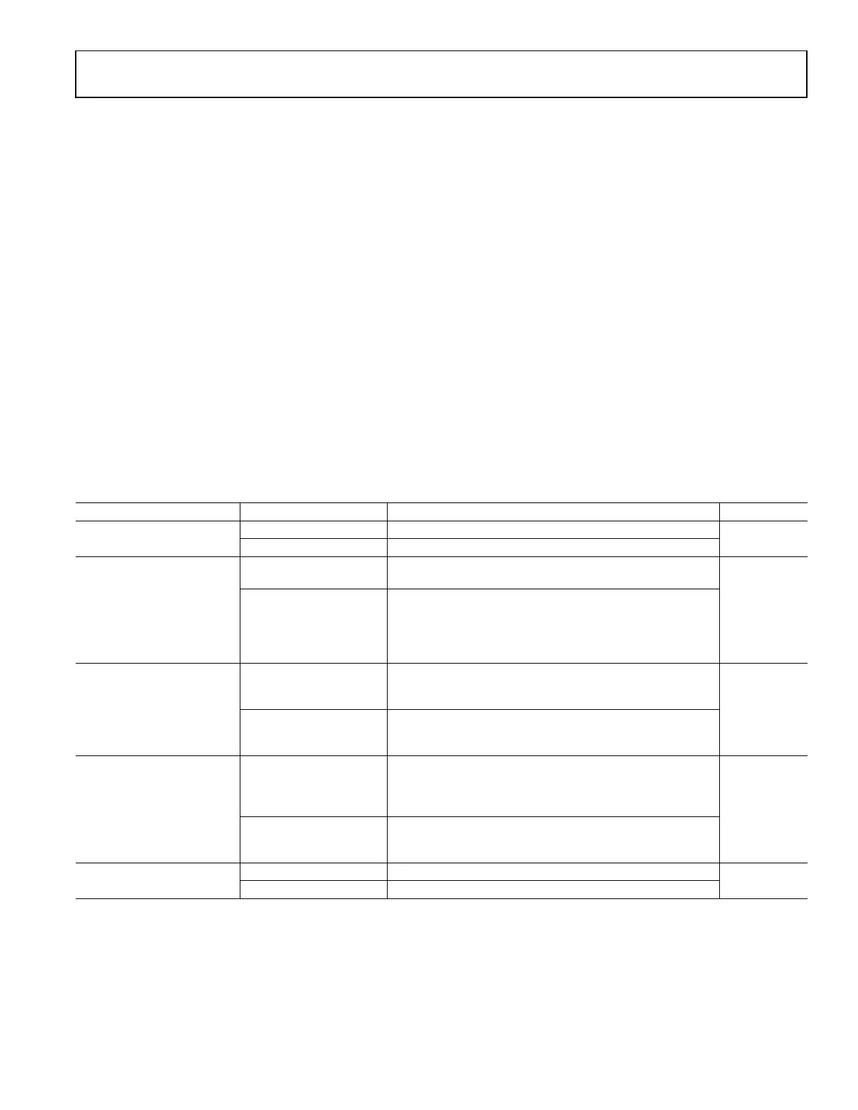
Table 15. CSSI Electrical Specification
Symbol Parameter Min Typ Max Units
VDIGIO_1P8 Interface power supply voltage 1.71 1.8 1.89 V
V
IH
Input voltage high VDIGIO_1P8 × 0.65 VDIGIO_1P8 + 0.18 V
V
IL
Input voltage low 0 VDIGIO_1P8 × 0.35 V
V
OH
Output voltage high VDIGIO_1P8 − 0.45 VDIGIO_1P8 V
V
OL
Output voltage low 0 0.45 V
f
CLK
Clock frequency 80 MHz
C
L
@ 80 MHz
Load capacitance supported for
an 80 MHz clock waveform
10 30 pF
Table 16. LSSI Electrical Specification
Symbol Parameter Conditions Min Typ Max Units
VDIGIO_1P8 Interface power supply voltage 1.71 1.8 1.89 V
V
I
Input voltage range 825 1675 mV
Input Common Mode Voltage 925 1200 1575 mV
V
IDTH
Input differential threshold −100 +100 mV
R
IN
Receiver differential input impedance 100 Ω
V
OH
Output voltage high R
LOAD
= 100 Ω ± 1% 1390 mV
V
OL
Output voltage low R
LOAD
= 100 Ω ± 1% 1000 mV
|V
OD
| Output differential voltage R
LOAD
= 100 Ω ± 1% 360 mV
V
OS
Output offset voltage R
LOAD
= 100 Ω ± 1% 1150 1200 1250 mV
R
O
Output impedance, single ended 80 100 120 Ω
I
SA
, I
SB
Output current Driver shorted to ground 17 mA
I
SAB
Output current Drivers shorted together 4.1 mA
Clock signal duty cycle 500 MHz 45 50 55 %
T
R
,T
F
Output Rise/Fall Time 300 mVp swing 0.371 nsec
CMOS SYNCHRONOUS SERIAL INTERFACE (CMOS-SSI)
One-Lane Mode CSSI Interface
Receive CSSI Interface
The one-lane mode receive CSSI interfaces of each channel (Rx1 and Rx2) are a 3-wire digital interface consisting of:
• RX_DCLK_OUT: is an output clock synchronizing data and strobe output signals.
• RX_STROBE_OUT: is an output signal indicating the first bit of the serial data sample.
• RX_DATA_OUT: is an output serial data stream.
The I and Q samples are serialized out starting with configurable I or Q first and MSB or LSB first, Figure 25 illustrates the receive CSSI
interface (Rx1 and Rx2) for a 16-bit I/Q data sample with I sample and MSB first configuration.
RX_DATA_OUT
RX_DCLK_OUT
R
X_STROB
E_OUT
OR
RX_STR
OBE_OUT
I0_D15 I0_D14 I0_D0 Q0_D15 Q0_D14 I0_Q0 I1_D15
24159-025
Figure 24. Receive CSSI Timing for 16-Bit I/Q Data Sample (I and MSB First)
The RX_STROBE_OUT signal is aligned with the first bit of the serialized data (I and Q), and can be configured to be high:
For one clock cycle at start of I and Q sample transmit. In the case a 16-bit data sample, RX_STROBE is high for one clock cycle and low
for 31 clock cycles.
 Loading...