UG-1828 Preliminary Technical Data
Rev. PrC | Page 282 of 338
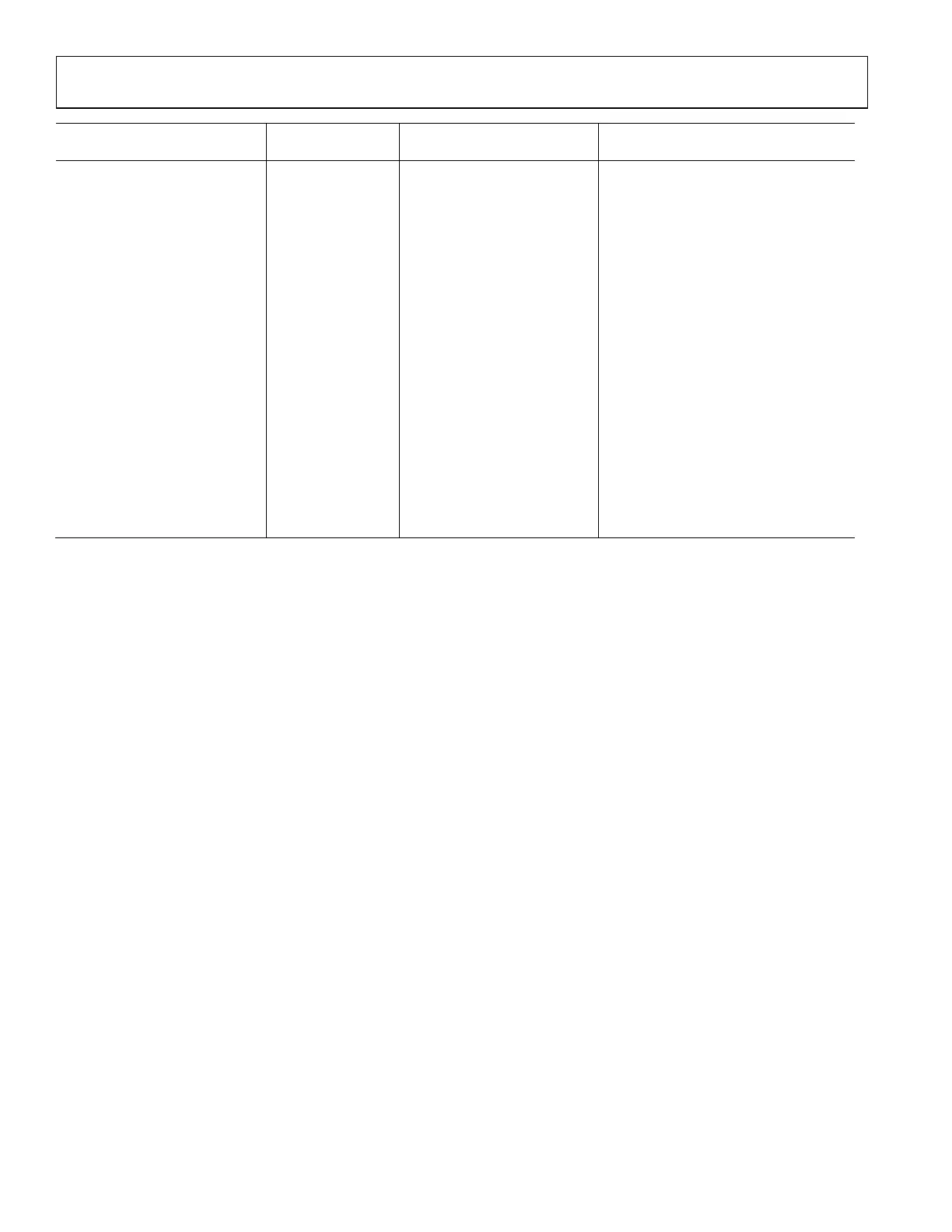
Pin No. Type Mnemonic Unused instructions
N7, N8, P1, P14 Input VSSD Not applicable.
N9 Input TX1_DCLK_IN- Do not connect
N10 Input TX1_DCLK_IN+ Do not connect.
N12 Output RX1_QDATA_OUT- Do not connect
N13 Output RX1_STROBE_OUT+ Do not connect
N14 Output RX1_STROBE_OUT- Do not connect
P2 Input TX2_STROBE_IN+ Do not connect
P3 Input/Output TX2_STROBE_IN- Do not connect
P4 Input TX2_QDATA_IN- Do not connect
P5 Input TX2_QDATA_IN+ Do not connect
P6 Input TX2_IDATA_IN+ Do not connect
P7 Input TX2_IDATA_IN- Do not connect
P8 Input TX1_IDATA_IN- Do not connect
P9 Input TX1_IDATA_IN+ Do not connect
P10 Input TX1_QDATA_IN+ Do not connect
P11 Input TX1_QDATA_IN- Do not connect
P12 Input/Output TX1_STROBE_IN- Do not connect
P13 Input TX1_STROBE_IN+ Do not connect
SUMMARY
Circuit board layout and power supply decoupling recommendations covered in this document are the recommendations of the Analog
Devices applications engineering team. These recommendations are based on circuit analysis, simulation, best practice layout techniques,
and experience with this and other transceiver devices. Designers are strongly encouraged to follow these guidelines carefully when
developing their own PCB applications. Deviation from these recommendations could result in sub-standard system performance that is
very difficult to isolate after the system has been committed to a PCB design. Contact Analog Devices for demo board layout files and
schematics that utilize many of the recommended techniques.
 Loading...