UG-1828 Preliminary Technical Data
Rev. PrB | Page 22 of 277
ADRV9001 IN FDD TYPE REPEATER APPLICATION
SPI
RESET
DEV_CLKL_OUT
MCS
DEV_CLK
DGPIOs
Rx/Tx_ENABLE
GP_INT
VGA
BPF FILTER
LNA
PA
LPF
BPF FILTER
LNA
ATTENUATOR
COUPLER
DUPLEXER
DUPLEXER
ANTENNA A
ANTENNA B
A
B
B
A
VCXO
BALUN
BALUN
BALUN
BALUN
BALUN
POWER IC
BALUN
BALUN
/2
SSI
DAC
BALUN
BALUN
VGA
PA
LPF
ATTENUATOR
COUPLER
FUNCTIONALITY
RECEPTION OF RF BAND B
USED BY Tx1 INIT CALIBRATIONS
RECEPTION OF RF BAND A
USED BY Tx2 INIT CALIBRATIONS
TRANSMISSION OF RF BAND A
TRANSMISSION OF RF BAND B
RF I/O
Rx1A
Rx1B
Rx2A
Rx2B
Tx1
Tx2
ADRV9001
FPGA
OR
BBIC
VDDA_1P0
VDDA_1P3
VDDA_1P8
VDD_1P0
VDD_1P8
RF PLL2
RF PLL1
/2
EXT LO2
EXT LO1
Tx1
Rx1A
Rx1B
Rx2A
Rx2B
Tx2
INT
QEC
LOL
Tx1
DATA
ADC
DDC
DEC
QEC
DC
SSI
Rx1
DATA
ADC
DDC
DEC
QEC
DC
SSI
Rx2
DATA
SSI
DAC
INT
QEC
LOL
Tx2
DATA
AuxDACAuxADC
AGPIOs
3/4/6/7/8/10
3/6/8
12/16
4
3/4
3/6/8
3/4/6/7/8/10
24159-009
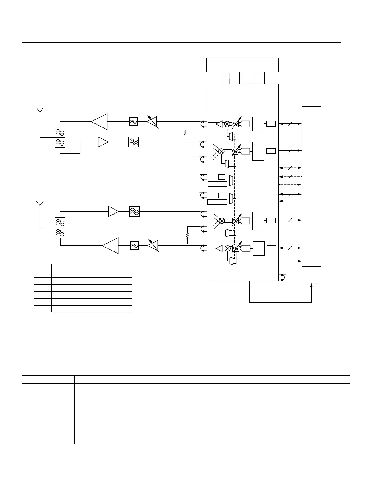
Figure 9. ADRV9001 in FDD Type Repeater Application with Baseband Processor Analyzing Traffic Data
ADRV9001 in FDD Type Repeater Application with Baseband Processor
With a minimum number of external components, the ADRV9001 transceiver can be used to build complete RF-to-bits signal chain that
can serve as RF front end in repeater or frequency translator type applications. ADRV9001 internal AGC can be used to autonomously
monitor and set the appropriate gain level for Rx signal chains. For none time critical FDD type applications control of the ADRV9001
TRx can be done thru API commands that use SPI interface.
Table 7. Constrains and Limitations in FDD Type Repeater Application with Baseband Processor Analyzing Traffic Data
Functionality Constrains and Limitations
Rx Signal Path
The user must ensure that appropriate level of isolation between Rx1 and Rx2 as well as Rx to Tx is provided at the
system level. In the previously described example, RxB inputs are used only during initialization calibrations. The user
must ensure that appropriate attenuation is present in line to prevent Rx being overloaded by Tx signal.
Tx Signal Path
The user must ensure that appropriate level of isolation between Tx1 and Tx2 as well as Rx to Tx is provided at the system
level.
LO Generation
In FDD type Repeater application, ADRV9001 can use its internal LO to generate RF LO1 for uplink (example: Tx1 and
Rx1) and RF LO2 for downlink (example: Tx2 and Rx2). It is also possible to use external LO inputs in this mode of
operation. External LO1 operating at 2× RF LO can be used for uplink and External LO2 operating at 2× RF LO can be
used for downlink.