Preliminary Technical Data UG-1828
Rev. PrB | Page 227 of 277
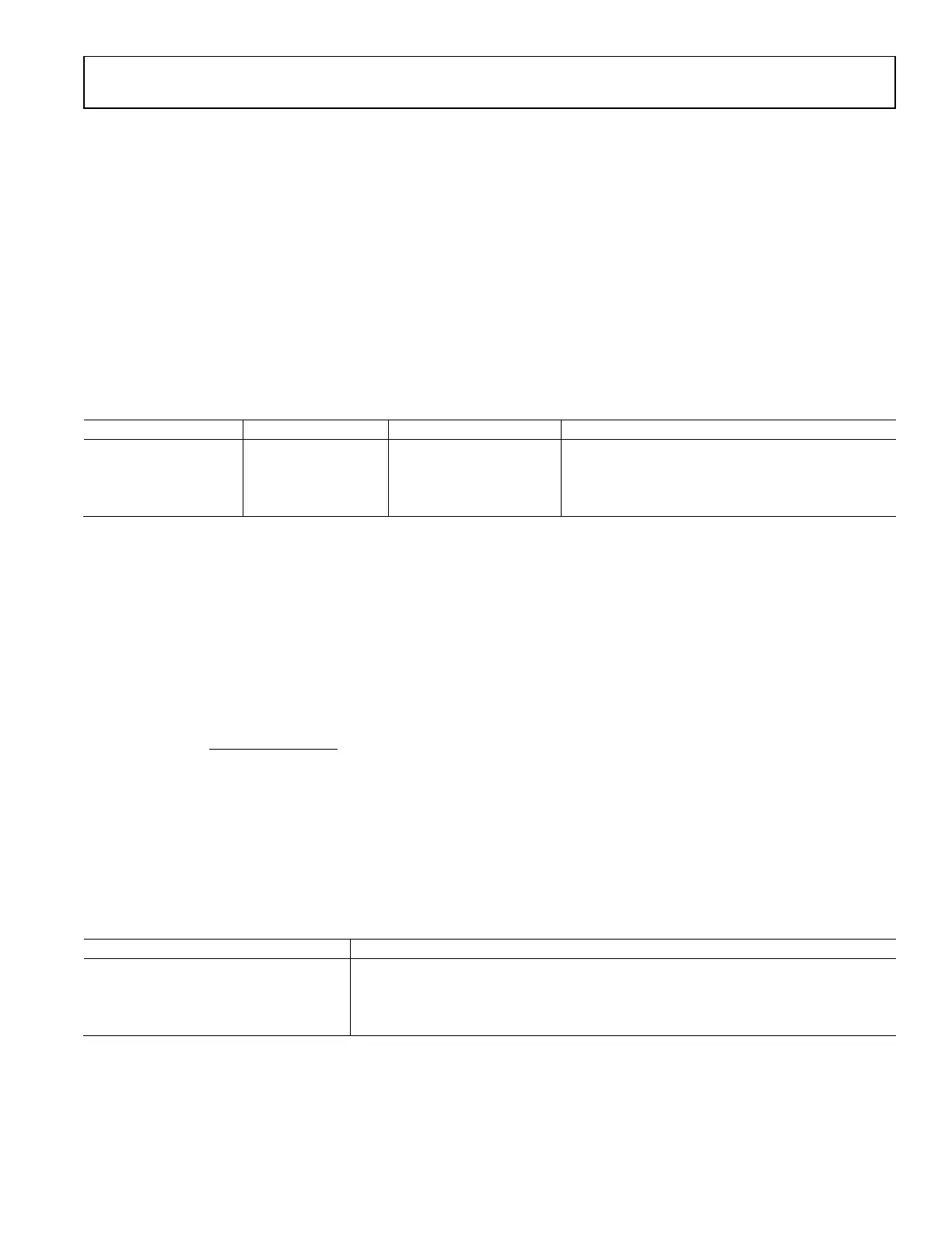
Figure 222. Layout Example of Power Supply Connections Routed with Ground Shielding (Layer 3)
Figure 222 shows an example of how the ferrite beads, reservoir capacitors and decoupling capacitors should be placed.
Recommendation is to connect a ferrite bead between a power plane and ADRV9001 at a distance away from ADRV9001. The ferrite
bead should supply a trace with a reservoir capacitor connected to it. That trace should then be shielded with ground and provide power
to ADRV9001 Power pin. A 1 µF capacitor should be placed near the power supply pin with the ground side of the bypass capacitor
placed so that ground currents flow away from other power pins and their bypass capacitors.
SEPARATE TRACE
SURROUNDED BY GROUND
FERRITE
BEAD
100µF
RESERVOIR
CAPACITOR
1µF BYPASS
CAPACITOR
AGND
C1043
1µF
VRX2LO_1P3
C1042
100µF
R1011
0Ω
VDDA_1P3
VDDA_1P0
R1012
DNI
2 1
1
E1024
120Ω
TP1024
RED
VIA TO
POWER
DOMAIN
BALL
Figure 223. Placement Example of Ferrite Beads, Reservoir and Bypass Capacitors on ADRV9001 Customer Card
(Layers: TOP, 3-Power and BOTTOM)
There are two possible power supply architectures for ADRV9001 transceivers, as follows:
• High performance, low risk, four power domains
• 1.8 V digital
• 1.8 V analog
• 1.3 V analog
• 1.0 V digital
 Loading...