UG-1828 Preliminary Technical Data
Rev. PrB | Page 50 of 277
RX_DATA_OUT
RX_DCLK_OUT
RX_STROBE_OUT
OR
RX_STROBE_OUT
S0_D15 S0_D14 S0_D8 S0_D7 S0_D6 S0_D0 S1_D15
24159-031
Figure 30. Receive CSSI Timing for 16-Bit Symbols (MSB First)
Figure 32 illustrates the transmit CSSI interface (Tx) for a 16-bit data symbols.
TX_DATA_IN
TX_DCLK_IN
TX_S
TRO
BE_IN
OR
TX_S
TRO
BE_IN
S0_D15 S0_D14
S0_D8 S0_D7 S0_D6 S0_D0
S1_D15
TX_DCLK_OUT
24159-032
Figure 31. Transmit CSSI Timing for 16-Bit Symbols (MSB First)
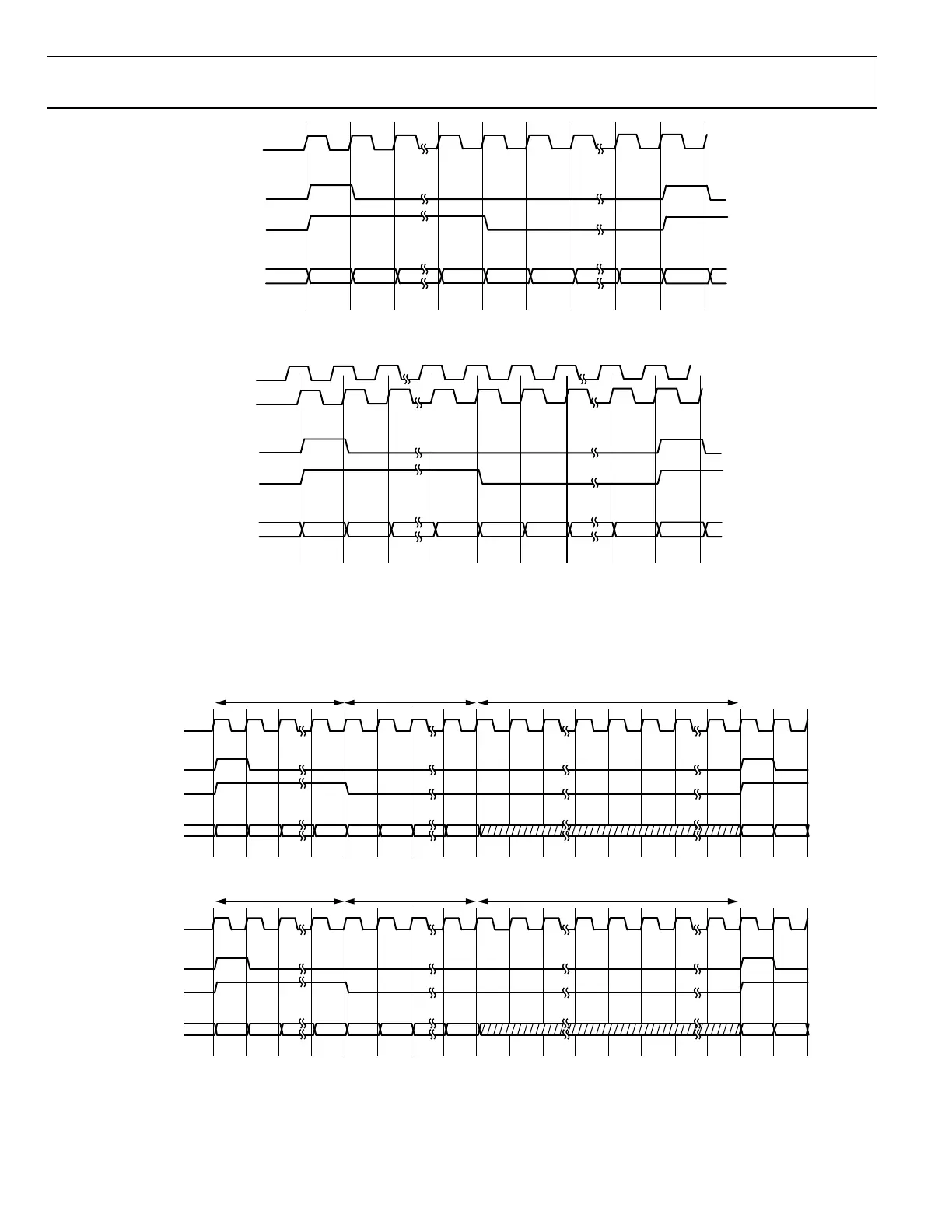
Receive CSSI Interface with 2×, 4×, and 8× Data Clock Rates
ADRV9001 receive CSSI supports the 2 times, 4 times, or 8 times of the data clock rate for some applications.
Figure 32, Figure 33, and Figure 34 illustrate the receive CSSI interface (Rx1 and Rx2) for 16-bit I/Q data sample with 2×, 4×, and 8×
clock rates. The strobe pulse validates the start of the 32-bit I and Q samples, the remaining data bits are ignored.
RX_DCLK_OUT
RX_STROBE_OUT
OR
RX_STROBE_OUT
RX_DATA_OUT
16 CYCLES (I SAMPLE) 16 CYCLES (Q SAMPLE)
32 CYCLES (NO SAMPLE)
I0_D15 I0_D14 I0_D0 Q0_D15
Q0_D14 Q0_D0 I0_D14I1_D15
24159-033
Figure 32. Receive CSSI Timing with 2× Data Clock Rate for 16-Bit I/Q Data Sample (MSB First), 32 Cycles
RX_DCLK_OUT
RX_STROBE_OUT
OR
RX_STROBE_OUT
RX_DATA_OUT
16 CYCLES (I SAMPLE) 16 CYCLES (Q SAMPLE) 96 CYCLES (NO SAMPLE)
I0_D15 I0_D14 I0_D0 Q0_D15 Q0_D14 Q0_D0 I0_D14I1_D15
24159-034
Figure 33. Receive CSSI Timing with 4× Data Clock Rate for 16-Bit I/Q Data Sample (MSB First), 96 Cycles
 Loading...