UG-1828 Preliminary Technical Data
Rev. PrB | Page 54 of 277
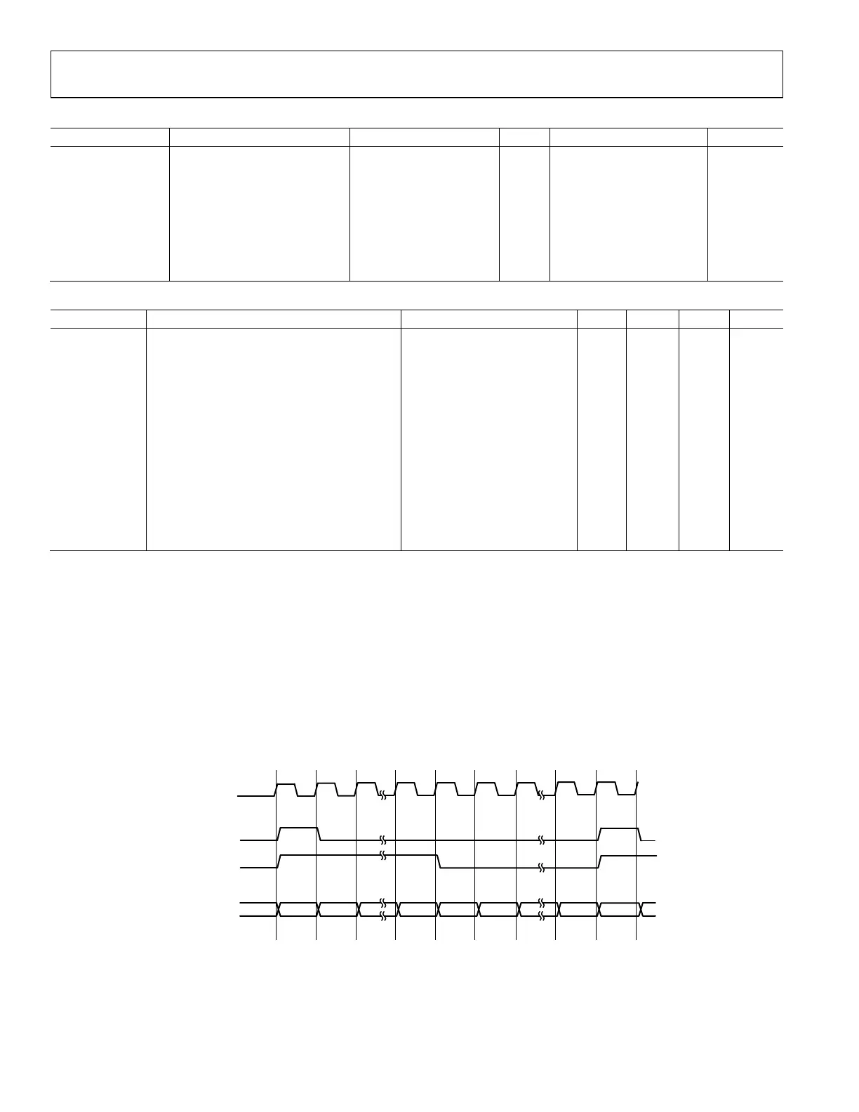
TX_IDATA0_IN
TX_DCLK_IN
OR
TX_DCLK_IN
TX_DCLK_OUT
TX_S
T
RO
BE_IN
OR
TX_S
TR
O
BE_IN
I0_D7 I0_D6
I0_D5 I0_D4
I0_D3
I0_D2 I0_D1
I0_D0 I1_D7
TX_IDATA1_IN
I0_D15 I0_D14 I0_D13 I0_D12
I0_D11 I0_D10 I0_D9 I0_D8 I1_D15
TX_QDATA2_IN
Q0_D7 Q0_D6 Q0_D5
Q0_D4 Q0_D3 Q0_D2 Q0_D1 Q0_D0 Q1_D7
TX_QDATA3_IN
Q0_D15
Q0_D14 Q0_D13
Q0_D12 Q0_D11 Q0_D10 Q0_D9
Q0_D8 Q1_D15
24159-044
Figure 43. Four-Lane Mode Transmit CSSI DDR Timing for 16-Bit I/Q Data Sample
LVDS SYNCHRONOUS SERIAL INTERFACE (LVDS-SSI)
Receive LSSI Interface
The LSSI receive interfaces of each channel (Rx1 and Rx2) are a 8-wire LVDS interface consisting of:
• RX_DCLK_OUT (±): is a differential output clock.
• RX_STROBE_OUT (±): is a differential output signal indicating the first bit of the serial data sample.
• RX_IDATA_OUT (±): is a differential output serial I data stream.
• RX_QDATA_OUT (±): is a differential output serial Q data stream.
Receive LSSI Interface with Separate Lanes for I and Q
Figure 44 illustrates the receive LSSI interface (Rx1 and Rx2) for a 16-bit I/Q data sample with MSB first configuration. Figure 45
illustrates the receive LSSI interface for a 12-bit I/Q data sample.
RX_IDATA_OUT+/–
RX_DCLK_OUT+
OR
RX_DCLK_OUT+
RX_
STR
OBE_OUT+
OR
RX_STROBE_OUT+
I0_D15
RX_QDATA_OUT+/–
Q0_D15 Q0_D7 Q0_D0 Q1_D15 Q1_D14Q0_D8
I0_D7 I0_D0 I1_D15 I1_D14I0_D8
24159-045
Figure 44. Receive LSSI Timing for 16-Bit I/Q Data Sample over Two Lanes (MSB First)
 Loading...