Preliminary Technical Data UG-1828
Rev. PrB | Page 55 of 277
RX_IDATA_OUT+/–
RX_DCLK_OUT+
OR
RX_DCLK_OUT+
RX_STROB
E_OUT+
OR
RX_
ST
R
OBE_OUT+
I0_D11
RX_QDATA_OUT+/–
Q0_D11 Q0_D5 Q0_D0 Q1_D11
Q1_D10
Q0_D6
I0_D5 I0_D0 I1_D11 I1_D10I0_D6
24159-046
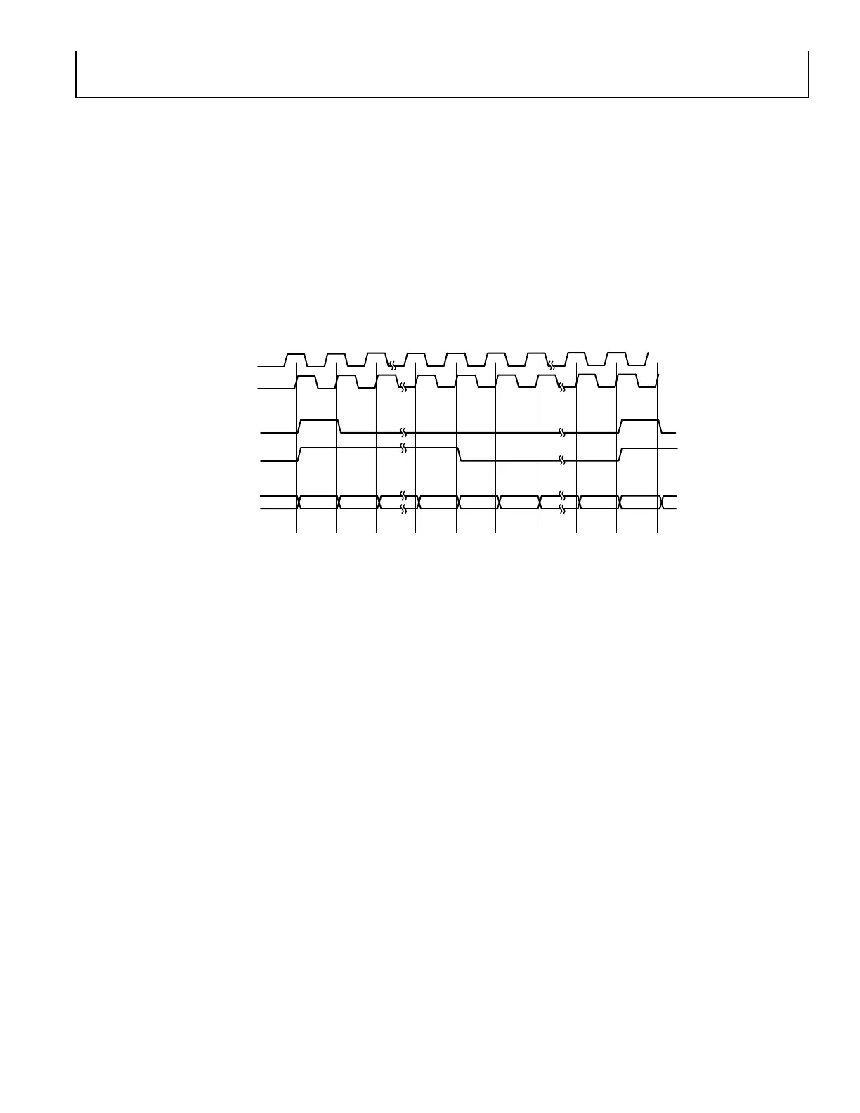
Figure 45. Receive LSSI Timing for 12-Bit I/Q Data Sample over Two Lanes (MSB First)
The RX_STROBE signal is aligned with the first bit of the serialized data (I and Q), and can be configured to be high:
• For a half clock cycle at the start of I and Q sample transmit. In the case of a 16-bit data sample, RX_STROBE is high for a half
clock cycle and low for a half and 15 clock cycles. In the case of a 12-bit data sample, RX_STROBE is high for a half clock cycle and
low for a half and 11 clock cycles.
• For half of I and Q data duration. In the case of a 16-bit data sample, the RX_STROBE is high for 4 clock cycles, and low for 4 clock
cycles (Q data sample). In the case of a 12bit data sample, the RX_STROBE is high for 3 clock cycles and low for 3 clock cycles.
In 12-bit I/Q mode, 16-bit samples from the receive datapath are cut to 12 bits for LSSI, a configurable option for the user to choose the
12-bit is from LSB or MSB of the 16-bit sample data.
Receive LSSI Interface with One Lane for I and Q
In this mode, only one lane is used to transfer I and Q data samples. The I/Q data bits are serialized with configurable I or Q first and
MSB or LSB first. The STROBE signal can be configured to high for a half clock cycle to indicate the start of I and Q symbols or for half
of I and Q data duration to distinguish between I data and Q data.
Figure 46 illustrates the one-lane receive LSSI interface (Rx1 and Rx2) for a 16-bit I/Q data sample with I sample and MSB first
configuration.
RX_IDATA_OUT+/–
RX_DCLK_OUT+
OR
RX_DCLK_OUT+
RX_STROBE_OUT+
OR
RX_STROBE_OUT+
I0_D15
RX_QDATA_OUT+/–
Q0_D15 Q0_D0 I1_D15 I1_D14I0_D0
24159-047
Figure 46. Receive LSSI Timing for 16-Bit I/Q Data Sample over One-Lane (I and MSB First)
Transmit LSSI Interface
The transmit LSSI interface of each channel (Tx1 and Tx2) is an 8-wire digital interface consisting of:
• TX_DCLK_IN (±): is a differential input clock synchronized to the data and strobe inputs.
• TX_STROBE_IN (±): is a differential input signal indicating the first bit of the serial data sample.
• TX_IDATA_IN (±): is a differential input serial I data stream.
• TX_QDATA_IN (±): is a differential input serial Q data stream.
An additional port might be used as a reference clock for the baseband processor to generate above Transmit LSSI clock, Strobe and Data
signal, the user could use RX1_DCLK_OUT or RX2_DCLK_OUT as a reference clock if these clock frequencies are equal to the TX clock
frequency.
 Loading...