UG-1828 Preliminary Technical Data
Rev. PrB | Page 56 of 277
An optional LVDS port (alternative function of Digital GPIO) can also be configured as an output LVDS pad used as a reference clock
TX_DCLK_OUT (±) for the baseband processor, the user could use TX_DCLK_OUT to generate above LSSI clock, strobe and data
signal.
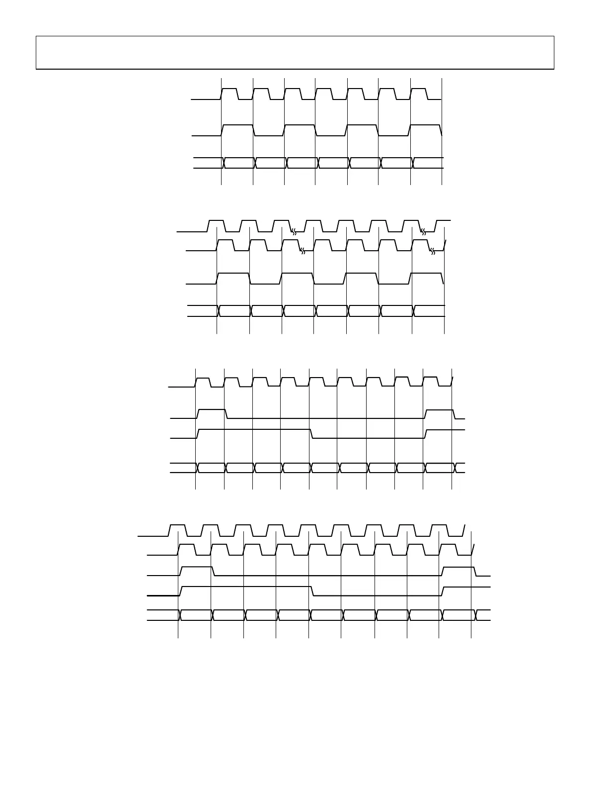
Transmit LSSI Interface with Separate Lanes for I and Q
Figure 47 illustrates the transmit LSSI interface (Tx1 and Tx2) for a 16-bit I/Q data sample with MSB first configuration.
TX_IDATA_IN+/–
TX_DCLK_IN+
OR
TX_DCLK_IN+
TX_DCLK_OUT+
TX_STROBE_IN+
OR
TX_STROBE_IN+
I0_D15
TX_QDATA_IN+/–
Q0_D15 Q0_D7 Q0_D0 Q1_D15 Q1_D14
Q0_D8
I0_D7 I0_D0 I1_D15 I1_D14I0_D8
24159-048
Figure 47. Transmit LSSI Timing for 16-Bit I/Q Data Sample on Separate Lanes
Figure 48 illustrates the Transmit LSSI interface (Tx1 and Tx2) for a 12-bit I/Q data sample with MSB first configuration.
TX_IDATA_IN+/–
TX_DCLK_IN+
OR
TX_DCLK_IN+
TX_DCLK_OUT+
TX_STROBE_IN+
OR
TX_STROBE_IN+
I0_D11
TX_QDATA_IN+/–
Q0_D11 Q0_D5 Q0_D0 Q1_D11 Q1_D10Q0_D6
I0_D5 I0_D0 I1_D11 I1_D10I0_D6
24159-049
Figure 48. Transmit LSSI Timing for 12-Bit I/Q Data Sample on Separate Lanes
The TX_STROBE signal is aligned with the first bit of the serialized data (I & Q), and can be configured to be high:
• For a half clock cycle at start of I and Q sample transmit. In the case a 16-bit data sample, the TX_STROBE is high for a half clock
cycle and low for a half and 15 clock cycles. In the case of a 12-bit data sample, the TX_STROBE is high for a half clock cycle and
low for a half and 11 clock cycles.
• For half of I and Q data duration. In the case of a 16-bit data sample, the TX_STROBE is high for 4 clock cycles, and low for 4 clock
cycles (Q data sample). In the case of a 12-bit data sample, the TX_STROBE is high for 3 clock cycles and low for 3 clock cycles.
In 12-bit I/Q mode, 12-bit samples from LSSI are extended to 16 bits by padding four bits zero in LSB for the following transmit datapath
process.
Transmit LSSI Interface with One Lane for I and Q
In this mode, only one lane is used to transfer I and Q data samples. The I/Q data bits can be deserialized with configurable I or Q first
and MSB or LSB first. The STROBE signal can be configured to high for a half clock cycle to indicate the start of I and Q symbols or for
half of I and Q data duration to distinguish when I Data and Q Data.
Figure 49 illustrates the one lane LSSI interface (Tx1 and Tx2) for a 16-bit I/Q data sample with I sample and MSB first configuration.
 Loading...