Preliminary Technical Data UG-1828
Rev. PrB | Page 57 of 277
TX_IDATA_IN+/–
TX_DCLK_IN+
OR
TX_DCLK_IN+
TX_DCLK_OUT+
TX_STROBE_IN+
OR
TX_STROBE_IN+
I0_D15
TX_QDATA_IN+/–
I0_D0 Q0_D15 Q0_D14 I0_Q0 I1_D15I0_D14
24159-050
Figure 49. Transmit LSSI Timing for 16-Bit I/Q Data Sample Sharing One Lane
POWER SAVING FOR LSSI
In TDD mode, the LVDS SSI pads can be powered down/up dynamically based on the Tx_Enable and Rx_Enable level to save power,
three LSSI power down modes are defined for different user’s requirement which are shown in Table 17. API
adi_adrv9001_Ssi_PowerDown_Set is used to set the power down mode for specified channel.
Table 17 LSSI power down mode
LSSI Power Down Mode Description
ADI_ADRV9001_SSI_POWER_DOWN_DISABLED All SSI PADS powered up in PRIMED
ADI_ADRV9001_SSI_POWER_DOWN_MEDIUM
RX_CLK and TX_REF_CLK SSI pads powered up,
TX_CLK and all STROBE and DATA SSI pads powered down in PRIMED
ADI_ADRV9001_SSI_POWER_DOWN_HIGH All SSI pads powered down in PRIMED
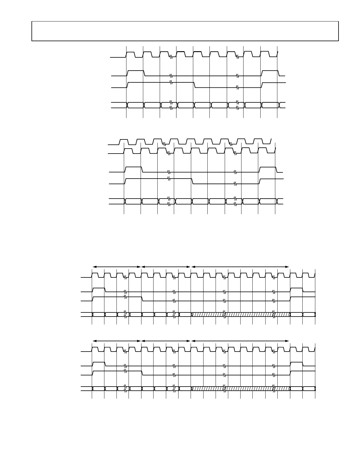
SSI TIMING PARAMETERS
Receive SSI and transmit SSI timing diagram are shown in Figure 50 and Figure 51. The preliminary timing specification for CMOS SSI
is described in Table 18 and the preliminary timing specification for LVDS SSI is described in Table 19.
DATA
CLOCK PERIOD
DATA
T
DELAY
RX_DCLK_OUT
RX_STROBE/DATA_OUT
T
DELAY
24159-051
Figure 50. Receive SSI Timing Diagram
DATA
CLOCK PERIOD
DATA
T
SETUP
T
HOLD
TX_DCLK_IN
TX_SROBE/DATA_IN
T
SETUP
T
HOLD
DATA
24159-052
Figure 51. Transmit SSI Timing Diagram
 Loading...