EasyManuals Logo

Analog Devices ADRV9002 User Manual

Analog Devices ADRV9002
338 pages
To Next Page IconTo Next Page
To Previous Page IconTo Previous Page
Page #249 background imageLoading...
Page #249 background image
Preliminary Technical Data UG-1828
Rev. PrC | Page 249 of 338
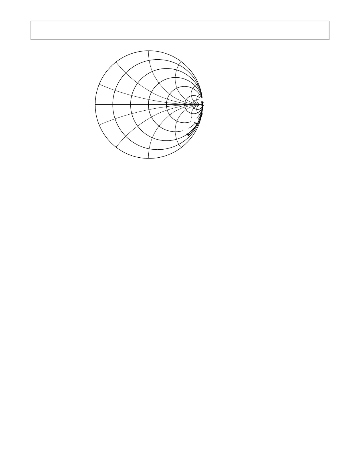
Figure 239. Device Clock Input Series Equivalent Differential Impedance
Device clock input board traces connected to device clock inputs balls should be implemented with stripline transmission lines using
inner copper layers in PCB stackup. The frequency of device clock input signal can go as high as 1GHz and stripline transmission line
approach will provide better signal integrity of clock signal especially at higher frequency as well as superior shielding of RF emission of
device clock signal.
The DEV_CLK_IN signal is available on the DEV_CLK_OUT pin. Table 102 describes default division applied to DEV_CLK_IN signal
after power up. Use can change this divider later on using API command. It should be noted that DEV_CLK_OUT pin is a CMOS type
pin with 80MHz of its maximum frequency of operation. It is intended to be used to provide clock to BBIC or on-board microcontroller
or audio CODEC type devices. It is not intended to be used by another RF sensitive IC.
For application where customer want to utilize internal RF LOs it is recommend to use 40MHz or above as a DEV_CLK frequency to get
the best in band phase noise.
There is a known issue with DEV_CLK input working in CMOS mode. When applied DEV_CLK input signal is in range between 10MHz
to 30MHz an internal RF LOs exhibit in band phase noise degradation of around 10dB .
If:
- this phase noise degradation is not acceptable and
- in customer end application it is mandatory to use DEV_CLK below 30MHz
then user should
- connect MODEA pin to GND which enables differential mode of operation for DEV_CLK input circuitry
- apply DEV_CLK as single ended to DEV_CLK_IN+ (E7 ball) and leave DEV_CLK_IN- (E8 ball) unconnected. Basically, the
same hardware configuration as in CMOS mode, outlined in Figure 237.
- ensure that amplitude of applied signal does note exceed 1V peak-to-peak. Signal in range of 400mW peak-to-peak is
recommended. The DEV_CLK_IN+ (E7 ball) inputs when operating in LVDS mode is biased on the device to around 200 mV
voltage level. Maximum of 400mV peak-to-peak amplitude ensures that the external clock stays compliant with electrical
specification of DEV_CLK_IN+ pin.
DEV_CLK_IN PHASE NOISE REQUIREMENTS
To prevent performance degradation, the DEV_CLK reference must be a very clean signal. Best performance from the synthesizer would
result if the applied reference were ideal, however that is unrealistic. Table 103 lists the required phase noise of the DEV_CLK signal for a
1dB system PN degradation compared to an ideal DEVICE CLOCK. For different DEV_CLK frequencies, the table can be scaled
appropriately. Clock source with phase noise performance outlined in Table 104 (or better) allows ADRV9001 to deliver datasheet
performance. It should be noted that Table 103 provide reference information for ADRV9001 operating with LTE type standards. Each
standard will determine its own DEV_CLK phase noise requirements. As an example, Table 104 provides recommendation for DEV_CLK
0
5.0
–5.0
2.0
1.0
–1.0
–2.0
0.5
–0.5
0.2
–0.2
m1
FREQUENCY = 10.00MHz
S(5,5) = 0.997/–402
IMPEDANCE = 9.694E3 + j2.467E4
m2
FREQUENCY = 100.0MHz
S(5,5) = 0.997/–4.067
IMPEDANCE = 137.890 – j2.809E3
m3
FREQUENCY = 300.0MHz
S(5,5) = 0.990/–12.133
IMPEDANCE = 46.714 – j938.620
m4
FREQUENCY = 600.0MHz
S(5,5) = 0.969/–23.831
IMPEDANCE = 36.427 – j471.206
m5
FREQUENCY = 1.000GHz
S(5,5) = 0.932/–38.422
IMPEDANCE = 32.096 – j283.752
FREQUENCY (100.0kHz TO 1.000GHz)
S(5,5)
M5
M3
M2
M1
M4
24159-189

Table of Contents

Questions and Answers:

Question and Answer IconNeed help?

Do you have a question about the Analog Devices ADRV9002 and is the answer not in the manual?

Analog Devices ADRV9002 Specifications

General IconGeneral
BrandAnalog Devices
ModelADRV9002
CategoryTransceiver
LanguageEnglish

Related product manuals