UG-1828 Preliminary Technical Data
Rev. PrB | Page 158 of 277
baseband processor. In this way, the device’s AGC can be used to react quickly to incoming blockers without the need for the baseband
processor to track the current gain index for the level of the received signal at the input to the device for signal strength measurements.
The digital gain block is controlled by the receiver gain table as mentioned earlier. Note different digital gain will be applied when
configured in gain correction or gain compensation mode. The receiver gain table has a unique front-end attenuator setting, with a
corresponding amount of digital gain, programmed at each index of the table, as shown in Table 53.
For the gain compensation mode, it can be used in either AGC or MGC mode. The digital gain allows for compensation of both the
internal analog attenuator and an external gain component (such as a DSA or LNA). After the digital gain compensation, the signal
power should only depend on the input signal power.
Around the end of the receiver datapath, receiver interface gain could be further applied by using a “Slicer” block for 2 major purposes.
One is to avoid digital saturation due to the bit-width limitation of the data port in gain compensation mode. The other one is to ensure
the overall SNR is limited only by analog noise and unaffected by quantization noise. When gain compensation mode is used, any analog
attenuation is compensated by a corresponding digital gain, such that the sum of the analog and digital gain is always equal to the
nominal receiver analog gain of 20 dB. At the ADC input, the full scale input signal is approximately 8.6 dBm. This value translates to 0
dBFS in the digital datapath for either the I or Q channel. As an example, assuming a 5dBm signal is applied at receiver input port, at the
receiver output, the signal power will be 5 + 20 = 25 dBm or 25 − 8.6 = 16.4 dBFS. This will cause clipping in 16-bit output signal.
Therefore, interface gain (less than 0 in this case) could be applied to attenuate the signal to avoid clipping. On the other hand, for a very
low signal level, at receiver input, within the RF bandwidth of interest, it must be assured that the analog noise dominates the
quantization noise. In the receiver datapath, the final 16-bit quantizer could become the dominant noise source as a result of the final
interface quantization. This quantization noise as a result of the final 16-bit quantizer will be spread over a bandwidth equivalent to its
output sampling frequency. For NB applications where the output sampling frequency is low, the total quantization noise per Hz could
be larger than the analog noise per Hz. By applying interface gain (greater than 0 in this case), prior to the final quantizer, the signal level
and analog noise level are both increased. Therefore, the analog noise dominates over the quantization noise so that SNR is dominated by
analog front-end noise in the RF bandwidth of interest. For WB applications, since the sampling frequency is higher, the total
quantization noise becomes much smaller. In such a case, the analog noise could be way above the quantization noise, therefore,
interface gain is not required.
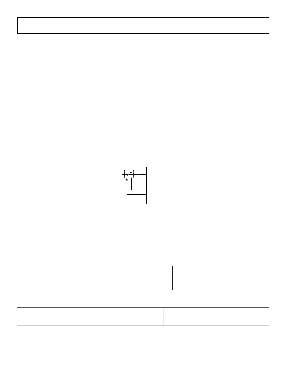
Figure 146 is a block diagram of the digital gain control portion of the Rx chain, showing the locations of the various blocks in the
simplified datapath.
WB/NB
DECIMATION
INTERFACE
GAIN
(SLICER)
LVDS/CMOS
MUX
API
RSSI
SIGNAL AFTER
HB FILTERING
DIGITAL
GAIN CONTROL
24159-120
Figure 147. Gain Control and Slicer Section of the Receiver Datapath
It can be seen from Figure 146 that digital gain control is performed in the WB/NB Decimation block. In NB and WB applications, the
digital gain control is actually performed at different stages of the receiver data chain to achieve optimal performance, which is simplified
in Figure 146. The slicer must be dependent on the desired signal power alone and must be done only when all the interfering signals
have been filtered out, for example, close to the end of the datapath. The Slicer operation can either be controlled automatically by the
device internally or by user externally through API commands. When controlled internally the RSSI block is used to determine the
amount of interface gain.
The following sections describe four different digital gain control modes in the device.
Mode 1: No Digital Gain Compensation with Internal Interface Gain Control
In this mode the digital gain block is used for gain correction. It applies a small amount of digital gain/attenuation to provide consistent gain
steps in a gain table. The premise is that because the analog attenuator does not have consistent steps in dB across its range then the digital gain
block can be used to even out the steps for consistency (the default table uses the digital gain block to provide consistent 0.5 dB steps).
With internal control, the device automatically applies the interface gain determined by RSSI, which measures the input signal power
right before the slicer. Note in the gain correction mode, interface gain less than 0 is not needed since the Rx output level should not
exceed 0 dBFS through either AGC or MGC. When in NB applications, the interface gain range could be from 0 dB to 18 dB in 6 dB step
size (0, 6, 12, 18) for improving the sensitivity. In WB applications, as discussed earlier, the sensitivity is already satisfied by the high
sampling rate so the interface gain is always 0.
 Loading...