UG-1828 Preliminary Technical Data
Rev. PrB | Page 194 of 277
Table 83 summarizes the available source control selections, source control is relevant for GPIO pins that are configured in the output
mode, GPIO pins operating in the input mode do not require a source control setup.
Table 83. Summary of Digital GPIO Output Features
Feature Description GPIO Pins Available for Feature
Control out Mux
Allows a choice of Main/RX/TX control signals to output from ADRV9001 to
monitor the status of the device
Any Digital GPIO
Manual Pin Toggle
Manual control the GPIO output level, API functions sets output pin levels
and reads the input pin levels
Any Digital GPIO
Monitor WakeUp
Baseband
Processor/DSP
Interrupt signal to wake up baseband processor/DSP when baseband
processor/DSP is in sleep state
Any Digital GPIO
Rx AGC overload
indicator
Allows output the AGC overload signals Any Digital GPIO
TX DCLK OUT
Allows output the SSI reference clock for baseband processor to generate the
TX SSI clock, data and strobe to ADRV9001
DGPIO_12 through DGPIO_13
TX Channel 1 SSI reference clock
out pin select,
DGPIO_14 through DGPIO_15
TX Channel 2 SSI reference clock
out pin select
Mirror Analog GPIO
Input
Allow the Analog GPIO input to output on Digital GPIO pins Any Digital GPIO
Control Out Mux
Control Out Mux (sometimes referred as “Monitor out”) allows status signals within the ADRV9001 to be output to digital GPIOs, such
as gain change flag, gain index, and Rx datapath overload detector status.
Manual Pin Toggle
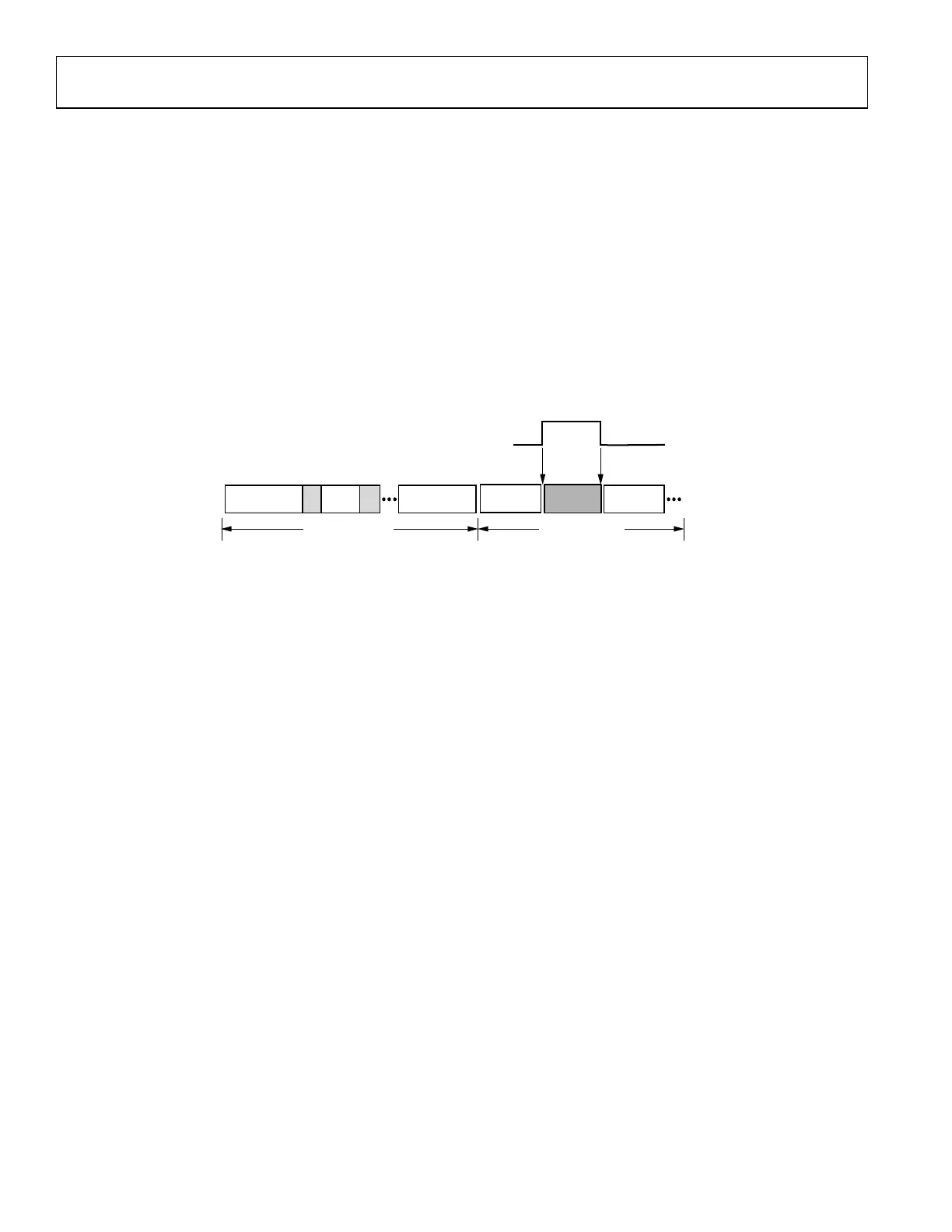
This feature allows control of the logic level of individual digital GPIO pins, after configuring the I/O direction and source control, the
adi_adrv9001_gpio_OutputPinLevel_Set() command is used to set the output level of GPIO pins.
adi_adrv9001_gpio_OutputPinLevel_Get() command is used to read the GPIO pins output levels.
Additionally, adi_adrv9001_gpio_InputPinLevel_Get() command can be used to read the input GPIO level if the relative GPIO is
configured as input.
Monitor Wake-Up Baseband Processor/DSP
Certain digital GPIO pin is assigned as “wake up baseband processor/DSP” to output the interrupt signal to wake up the baseband
processor/DSP when ADRV9001 works in monitor mode and specific detection conditions are met.
Rx AGC Overload Indicator
The status of peak detectors and power detector in the Rx channel can be retrieved to baseband processor through a set of DGPIO pins.
One DGPIO configuration is for using the peak detect mode, in which the overrange and under-range conditions of both APD and HB
detectors are provided to user. The other DGPIO configuration is for using the peak/power detect mode, in which the overrange and
underrange conditions of APD and power detector are provided to user.
The DGPIO pins could be associated with either one of the receivers, Rx1 or Rx2. However, when the similar information is required for
both receivers, they could be selectively muxed and provided to user simultaneously.
Data structure of adi_adrv9001_GainControlCfg_t, and of its substructures, adi_adrv9001_PeakDetector_t, adi_adrv9001_PowerDetector_t
initialize the necessary Gain control parameters as well as the digital GPIO pins assignment for the overload indicator, API command
adi_adrv9001_Rx_GainControl_Configure() is provided to set the parameters. (See the Receiver Gain Control section for details.)
TX DCLK OUT
This mode allows to configure the GPIO pins to a pair of differential or a single-ended reference clock for baseband processor if the TX
SSI and RX SSI runs at different lane rate, the users could use this reference clock to generate the TX LSSI clock, data and strobe when the
RX SSI and TX SSI run at different clock rate. TX1_DCLK_OUT± functionality can be assigned DGPIO_15 and DGPIO_14 when it is in
LVDS mode, or either of DGPIO_15 or DGPIO_14 can be used as the Tx1 SSI DCLK out if it is in CMOS mode. TX2_DCLK_OUT±
functionality can be assigned DGPIO_13 and DGPIO_12 when it is in LVDS mode, or either of DGPIO_13 or DGPIO_12 can be used as
the Tx1 SSI DCLK out if it is in CMOS mode.
 Loading...