UG-1828 Preliminary Technical Data
Rev. PrB | Page 18 of 277
ADRV9001 IN TETRA TYPE PORTABLE RADIO APPLICATION
SPI
RESET
DEV_CLKL_OUT
MCS
DEV_CLK
DGPIOs
Rx/Tx_ENABLE
GP_INT
BPF FILTER
LNA
ATTENUATOR
RF SWITCH
COUPLER
ANTENNA
VCXO
BALUN
BALUN
BALUN
BALUN
POWER IC
BALUN
BALUN
/2
SSI
DAC
VGA
PA
LPF
FUNCTIONALITY
RF RECEPTION
USED BY Tx DPD AND CALIBRATIONS
RF TRANSMISSION
RF I/O
Rx1A
Rx1B
ADRV9001
FPGA
OR
BBIC
VDDA_1P0
VDDA_1P3
VDDA_1P8
VDD_1P0
VDD_1P8
RF PLL2
RF PLL1
/2
EXT LO2
EXT LO1
Tx1
Rx1A
Rx1B
Tx1
DATA
ADC
DDC
DEC
QEC
DC
SSI
Rx1
DATA
AuxDACAuxADCAGPIOs
3/4/6/7/8/10
3/6/8
14/16
2
3/4
TEMPERATURE
SENSOR
EXTERNAL
LO SOURCE
Tx1
24159-007
INT
QEC
LOL
DPD
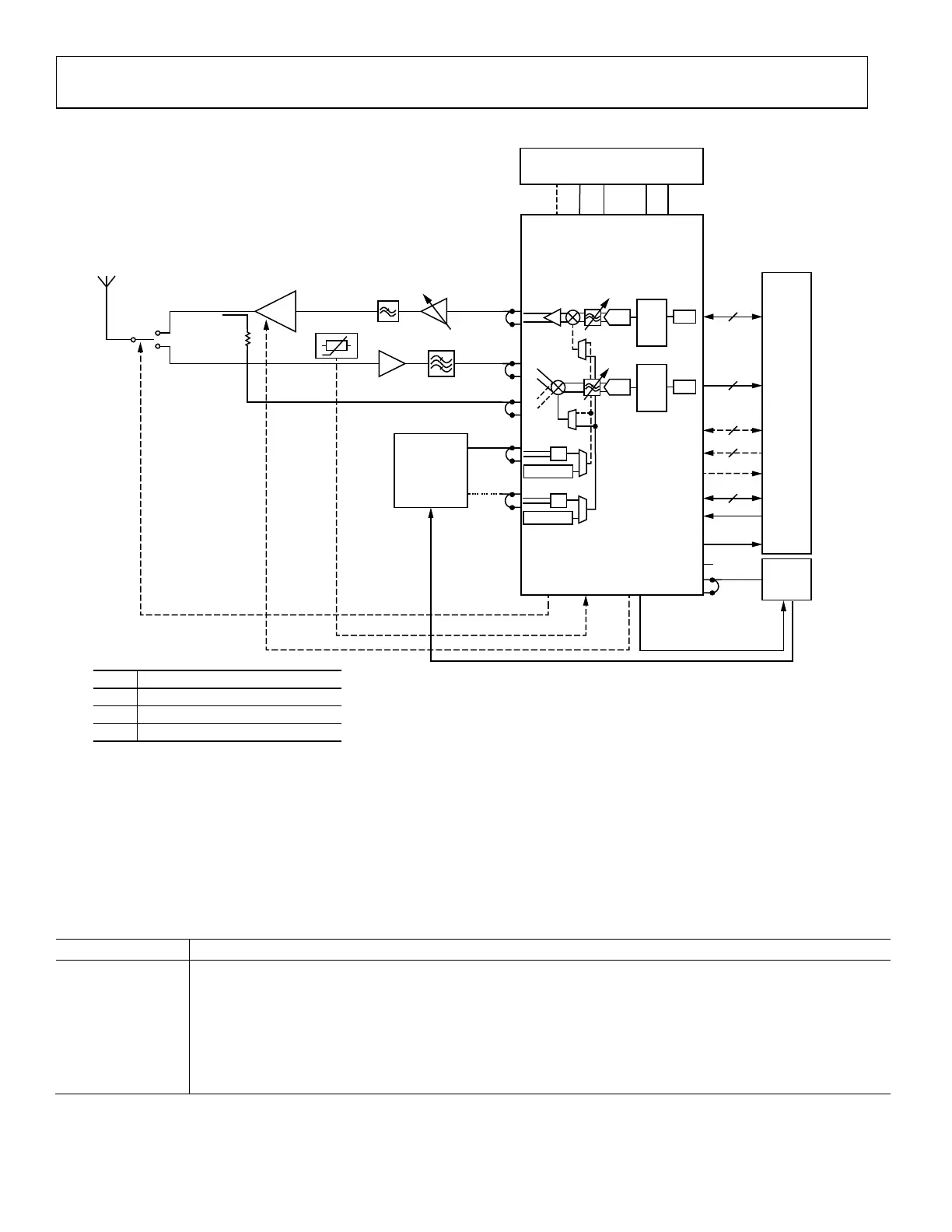
Figure 7. ADRV9001 in TETRA Type Portable Radio Application
TETRA Type Portable Radio Overview
With a minimum number of external components, the ADRV9001 transceiver can be used to build complete RF-to-bits signal chain that
can serve as RF front end in TETRA type applications. Internal DPD block can be used to linearize external power amplifier and improve
overall system efficiency. For systems that demand superior LO phase noise performance, ADRV9001 allows user to apply eternal RF
LO. ADRV9001 internal AGC can be used to autonomously monitor and set appropriate gain level for Rx signal chain. For time critical
TDD type applications control of the ADRV9001 TRx can be done by toggling control lines. ADRV9001 can control external Rx/Tx
switch using its analog GPIOs as well as provide power amplifier bias voltage by utilizing AuxDAC outputs.
Table 5. Constrains and Limitations in TETRA Type Portable Radio Application
Functionality Constrains and Limitations
LO Generation
In Portable Radio, TETRA type application, ADRV9001 can use its internal LO to generate RF LO1 for both uplink and
downlink. For applications with stringent RF LO requirements, the user can use external LO inputs. External LO1
operating at 2× RF LO can be used for both uplink and downlink.
RF Front End
For LO generation, the ADRV9001 uses internal VCO that generates a square wave type signal. A square wave LO
would produce harmonics. For example: depending of RF matching used on the RF ports user 2nd LO harmonic can
be as high as −50 dBc and 3rd harmonic can be as high as −9 dBc. Therefore, the RF filtering on the Rx and Tx path
must ensure that signals at the LO harmonic frequencies (up to 9th in some cases) are not affecting overall system
performance.
 Loading...