UG-1828 Preliminary Technical Data
Rev. PrB | Page 136 of 277
Gain Compensation
The process of compensating for the analog attenuation in the device (prior to the ADC) with a corresponding amount of digital gain
before the digital signal is sent to the user.
High Threshold
This threshold is used to trigger gain attack event. Some detectors could have multiple high thresholds.
Low Threshold
This threshold is used to trigger gain recovery event. Some detectors could have multiple low thresholds.
Threshold Overload
When a threshold is exceeded in a signal detector, this is referred to as an overload.
Threshold Underload
When a threshold is not exceeded in a signal detector, this is referred to as an underload.
Overrange Condition
An overrange condition exists when the AGC is required to reduce the gain. This can either be a peak condition, where a programmable
number of individual overloads of a high threshold have occurred within a defined period of time, or a power condition, where the
measured power exceeds a high power threshold.
Underrange Condition
An underrange condition exists when the AGC is required to increase the gain. This can either be a peak condition, where a lower
threshold is not exceeded a programmable number of times within a defined period of time, or a power condition, where the measured
power does not exceed a low power threshold.
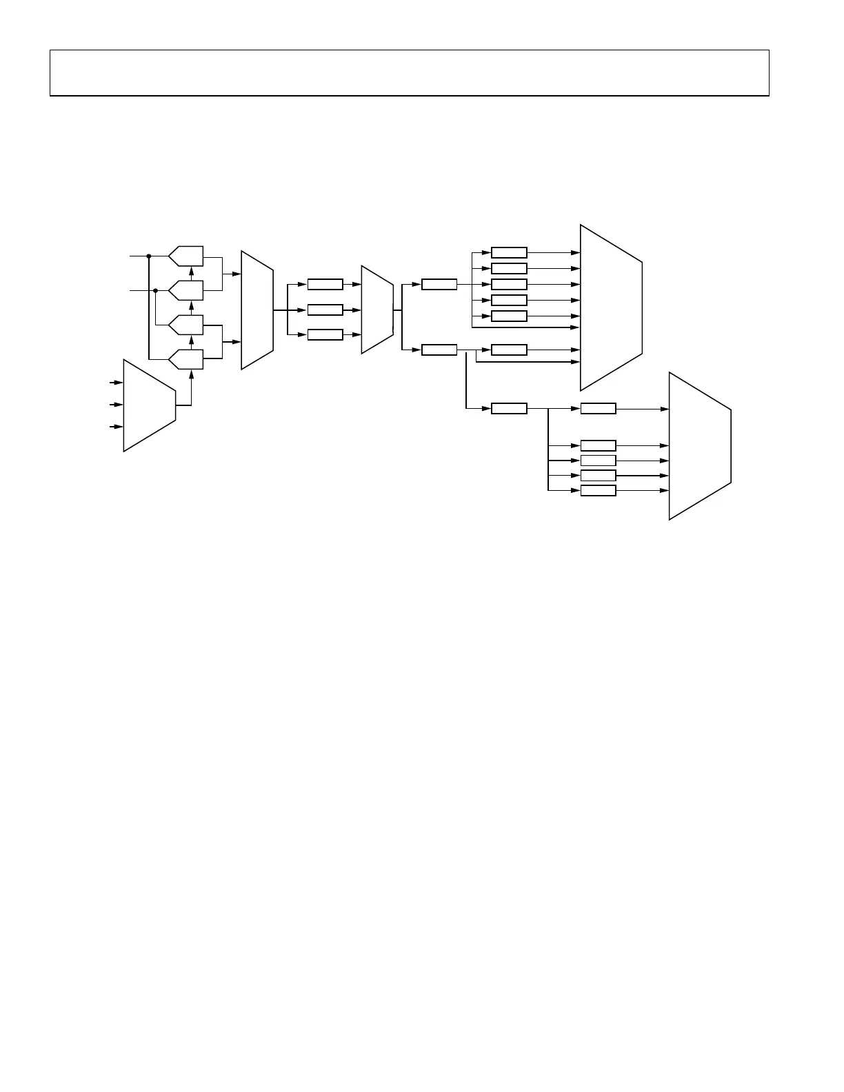
RECEIVER DATAPATH
Figure 132 shows the simplified receiver datapath and gain control blocks. The receivers have front end attenuators prior to the mixer
stage that are used to attenuate the signal in the analog domain to ensure the signal does not overload the receiver chain. Note
ADRV9001 provides about 20dB gain so the front end gain attenuator further attenuates signal from that level. In the digital domain,
there is also digital gain control capability.
As shown in this figure, the receiver chain has a number of observation elements that can monitor the incoming signal. These can be
used in either MGC or AGC mode. Firstly, an Analog Peak Detector (APD) exists prior to ADC. Being in the analog baseband, this peak
detector will see signals first, and will also have visibility of interfering signals which can overload the ADC but could be filtered as they
progress through the digital chain. The second peak detector is called the HB Peak Detector since it monitors the data at the output of the
Half Band (HB) Filtering block in the receiver chain.
A power measurement detection block is also provided at the same output of HB Filtering block which takes the RMS power of the
received signal over a configurable period of time.
Besides the front end gain control, this device could also control an external gain element through analog GPIO (AGPIO) pins (currently
not supported). In the digital domain, this device can further control the digital gain in both wideband (WB) and narrowband (NB)
modes. To avoid saturate the output signal due to the limitation of the bit width of data port, an optional interface gain (slicer) is applied
at the end of the datapath by properly shifting the data. The interface gain could be automatically controlled internally inside the device
by utilizing the information provided from the Receiver Signal Strength Indicator (RSSI) block or manually controlled by users through
API command.
As shown in Figure 132, the gain control block has multiple inputs, which come from 2 peak detectors the 1 power detector. By utilizing
the information from those detectors, the gain control block controls the gain of the signal chain using a predefined gain table. Note the
default gain table is loaded into the device during initialization. An API function adi_adrv9001_Rx_GainTable_Write() can be called by
the user to load a custom gain table or reconfigure the gain table. Note this operation should be done before performing initial
calibrations.
 Loading...