UG-1828 Preliminary Technical Data
Rev. PrB | Page 218 of 277
Figure 212. External LO1/ External LO2 Return Loss of Ext LO Port
Figure 213. External LO1/ External LO2 Insertion Loss, Simulated
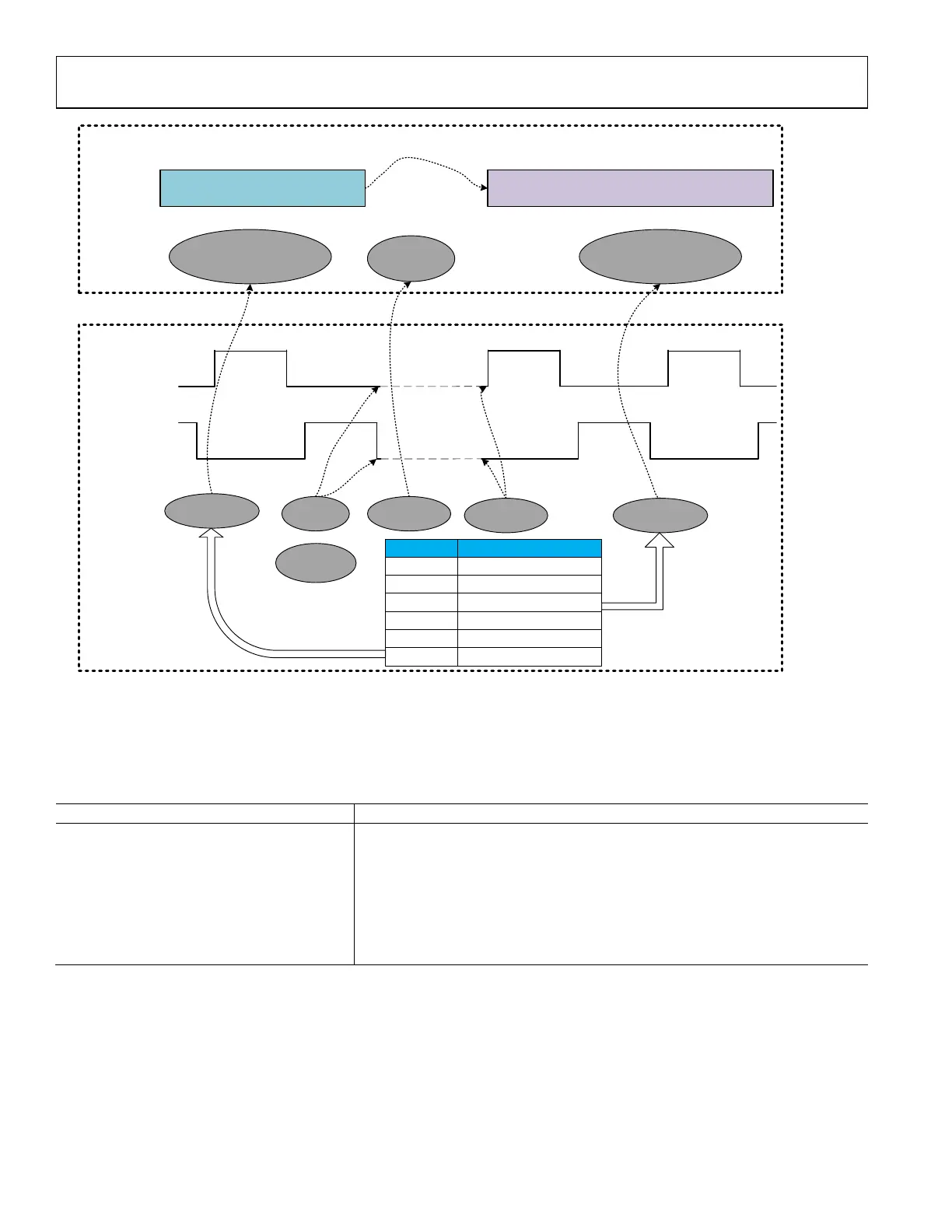
CONNECTION FOR EXTERNAL DEVICE CLOCK (DEV_CLK_IN)
ADRV9001 can accommodate 3 different types of external clock signals applied at device clock input pins. A differential low voltage
differential signalling (LVDS) clock signal or a single-ended clipped sinewave clock signal from a TCXO can be applied to the device
input pins. Furthermore, a crystal can be connected to device clock input pins to configure it as a crystal oscillator/driver by applying DC
voltage into MODEA pin as shown below.
 Loading...