UG-1828 Preliminary Technical Data
Rev. PrB | Page 106 of 277
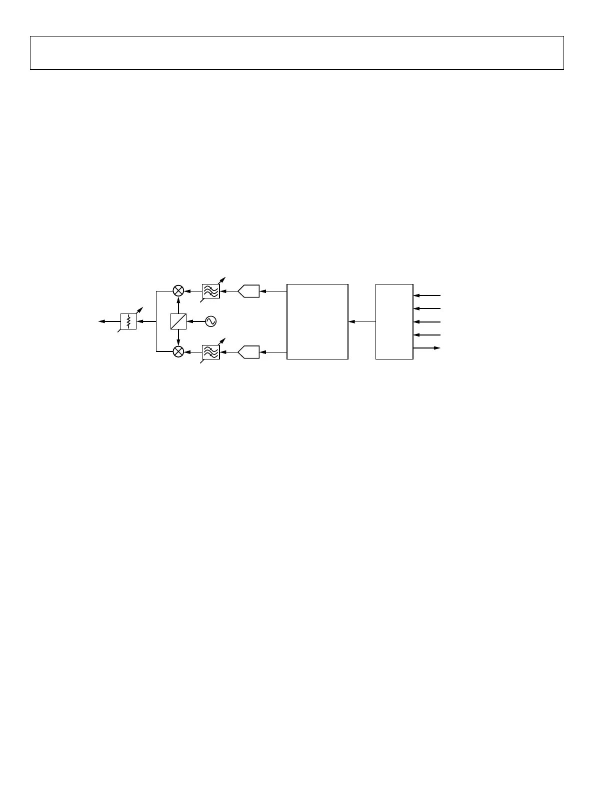
TRANSMITTER SIGNAL CHAIN
The ADRV9001 device integrates dual direct-conversion (Zero-IF) transmitters. It supports both time division duplexing (TDD) and
frequency division duplexing (FDD) modes and is capable of transmitting both narrowband (NB) and wideband (WB) signals. It
supports a wide range of applications such as DMR, P25 and TETRA as examples of NB standards and LTE as an example of WB
standards.
In general, each transmitter consists of an independent I and Q signal path with separate digital filters, DACs, analog transmit low pass
filters (LPF) and up-conversion mixers. After mixers, an analog attenuator is employed to control the transmitter output signal power.
Data from baseband processor is input to the transmitter signal path via synchronous serial interface (SSI). The serial data is converted to
parallel format through the deframer and then the data is processed by interpolation filters. There are several signal conditioning
functions, such as transmitter gain control, power amplifier protection, power amplifier, digital pre-distortion (DPD), transmitter
quadrature error correction (QEC) and transmitter LO leakage (LOL) handling, before the data is passed on to the DACs. The DAC
outputs are filtered by LPF, upconverted to RF via the mixer and attenuated through the analog attenuator to prepare for RF
transmission. The ADRV9001 device also supports FM/FSK modulation for some NB applications which will be discussed later.
The high level block diagram of the transmitter signal path is shown in Figure 113.
DAC
LPF
MIXER
ANALOG
ATTENUATOR
TX1/2
MIXER
DAC
LPF
90°
0°
INTERPOLATION
TX GAIN CONTROL
PA PROTECTION
DPD
TX LOL
TX QEC
FM MODUTATION
SERIAL
INTERFACE
TX1/2_IDATA_IN±
TX1/2_DCLK_OUT±
TX1/2_STROBE±
TX1/2_CLK_IN±
TX1/2_QDATA_IN±
24159-086
Figure 113. High Level Block Diagram of TX Signal Chain
DATA INTERFACE
The transmitter data interface supports several different interface rates and configurations. It has a total of 5 differential pairs (that is a
total of 10 wires). The interface is operated single-ended in CMOS synchronous serial interface (CSSI) mode and differential in LVDS
synchronous serial interface (LSSI) mode.
The CSSI interface has one or four data wires as well as one strobe, input and output clock wire. Depending on the number of data wires,
the data interface is referred to as CSSI one-lane or CSSI four-lane, respectively. The output clock is passed to the baseband processor to
generate the data, strobe and clock signals.
In one-lane operation, the I- and Q-symbols are interleaved and sequentially transmitted over the CSSI interface. Each symbol can
consist of 2, 8, or 16 bits. The four-lane interface only supports 16-bit symbols. They are separated into two 8-bit words for each I and Q
stream, and then sent over the 4 data wires of the CSSI four-lane interface.
For the LSSI interface, there is a separate data lane for the I- and Q-data. There is also a mode where the I-data and Q-data can be
interleaved and transferred over a single data lane. The bit-width of the data symbols can be 12 or 16 bits. In addition to the data lanes,
the interface has a strobe, an input clock and an optional output clock signal. The output clock signal can be used by the baseband
processor to generate the above data, clock and strobe signals.
As mentioned previously, the ADRV9001 supports many NB and WB standards. Depending on the selected standard and the specific
symbol rate chosen via the API profile, the interface clock rate can vary significantly. For the currently supported use cases, the interface
rate can range from 9.6 kHz to 983.04 MHz. Please note that the CSSI interface is a slow-speed interface and is not able to cover this
entire frequency range. Please refer to Data Interface section in this User Guide for more information.
 Loading...