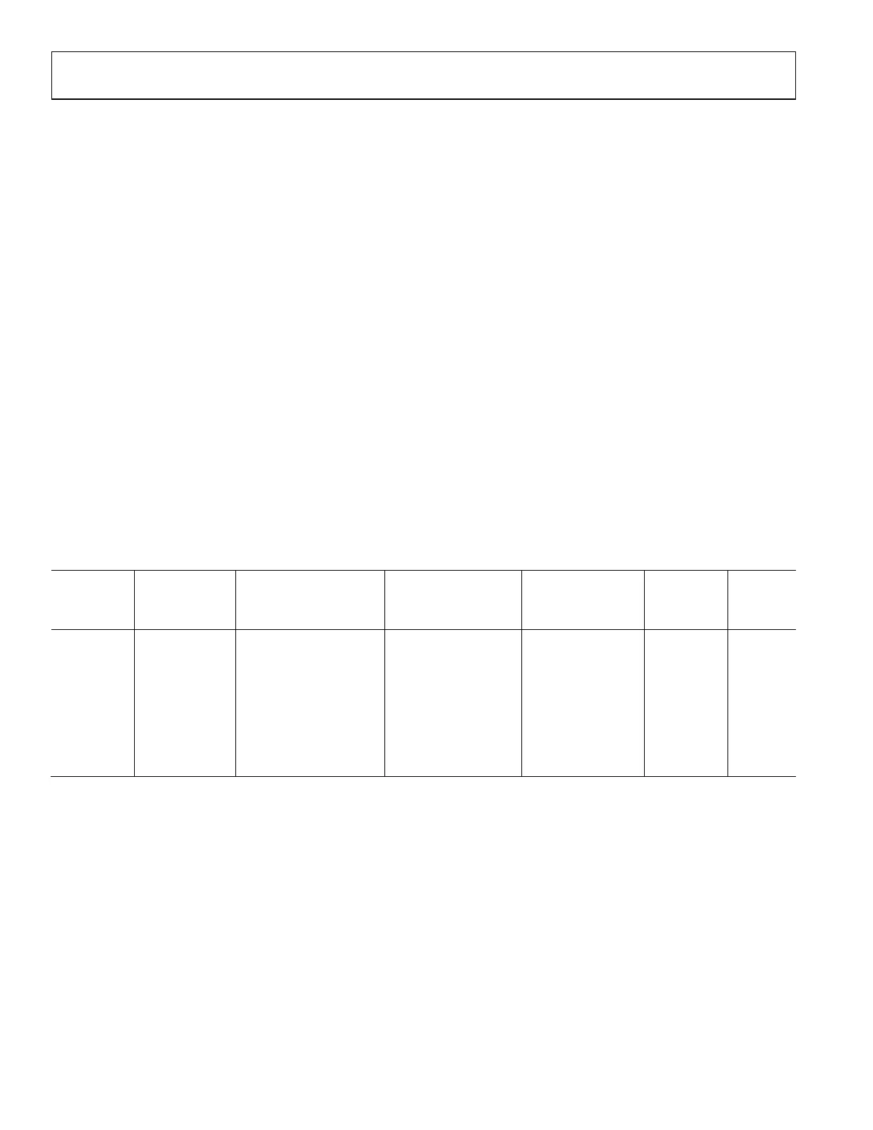
UG-1828 Preliminary Technical Data
Rev. PrB | Page 52 of 277
Figure 39 illustrates the receive CSSI interface (Rx1 and Rx2) for a four-lane format with MSB first configuration.
RX_IDATA0_OUT
RX_DCLK_OUT
R
X_
ST
R
OB
E_O
U
T
OR
RX_STROBE_OUT
RX_IDATA1_OUT
RX_QDATA2_OUT
RX_QDATA3_OUT
I0_D7 I0_D6 I0_D5 I0_D4 I0_D3 I0_D2 I0_D1 I0_D0
I1_D7
I0_D15 I0_D14 I0_D13 I0_D12 I0_D11 I0_D10 I0_D9 I0_D8 I1_D15
Q0_D7 Q0_D6 Q0_D5 Q0_D4 Q0_D3 Q0_D2 Q0_D1 Q0_D0 Q1_D7
Q0_D15 Q0_D14 Q0_D13 Q0_D12 Q0_D11 Q0_D10
Q0_D9 Q0_D8
Q1_D15
24159-039
Figure 38. Four-Lane Mode Receive CSSI Timing for 16-Bit I/Q Data Sample (MSB First)
The four-lane mode CSSI transmit interface of each channel (Tx1 and Tx2) is a 7-wire digital interface consisting of:
• TX_DCLK_IN: is an input clock synchronized to the data and strobe inputs.
• TX_STROBE_IN: is an input signal indicating the first bit of the serial data sample.
• TX_IDATA0_IN: is an input serial data stream of I sample low byte.
• TX_IDATA1_IN: is an input serial data stream of I sample high byte.
• TX_QDATA2_IN: is an input serial data stream of Q sample low byte.
• TX_QDATA3_IN: is an input serial data stream of Q sample high byte.
• TX_DCLK_OUT: is an optional output reference clock that is provided to the baseband processor to generate all the above signals,
the baseband processor can also RX_DCLK_OUT as the reference clock when its clock rate is equal with transmit SSI clock rate.
Figure 40 illustrates the transmit CSSI interface (Tx1 and Tx2) for a four-lane format with MSB first configuration.
TX_IDATA0_IN
TX_DCLK_IN
TX_DCLK_OUT
TX_STROBE_IN
OR
TX_STROBE_IN
I0_D7 I0_D6 I0_D5
I0_D4 I0_D3 I0_D2 I0_D1 I0_D0 I1_D7
TX_IDATA1_IN
I0_D15 I0_D14 I0_D13 I0_D12 I0_D11 I0_D10 I0_D9 I0_D8 I1_D15
TX_QDATA2_IN
Q0_D7 Q0_D6 Q0_D5 Q0_D4 Q0_D3 Q0_D2 Q0_D1 Q0_D0
Q1_D7
TX_QDATA3_IN
Q0_D15 Q0_D14 Q0_D13 Q0_D12 Q0_D11 Q0_D10 Q0_D9 Q0_D8 Q1_D15
24159-040
Figure 39. Four-Lane Mode Transmit CSSI Timing for 16-Bit I/Q Data Sample (MSB First)
Transmit and Receive CSSI Using DDR Clock
Transmit and receive CSSI can be operated in either SDR or DDR data transfer.
Figure 41 illustrates the Rx CMOS SSI interface with DDR clock in relation with strobe/data. Each edge of the clock (positive and
negative) corresponds to a data sample. The RX DDR Clock can be generated in phase with the data/strobe or delayed quarter cycle of
the clock period, the optional delayed clock helps to ease the timing interface of the baseband processor to meet the setup/hold on the
baseband processor).