UG-1828 Preliminary Technical Data
Rev. PrB | Page 188 of 277
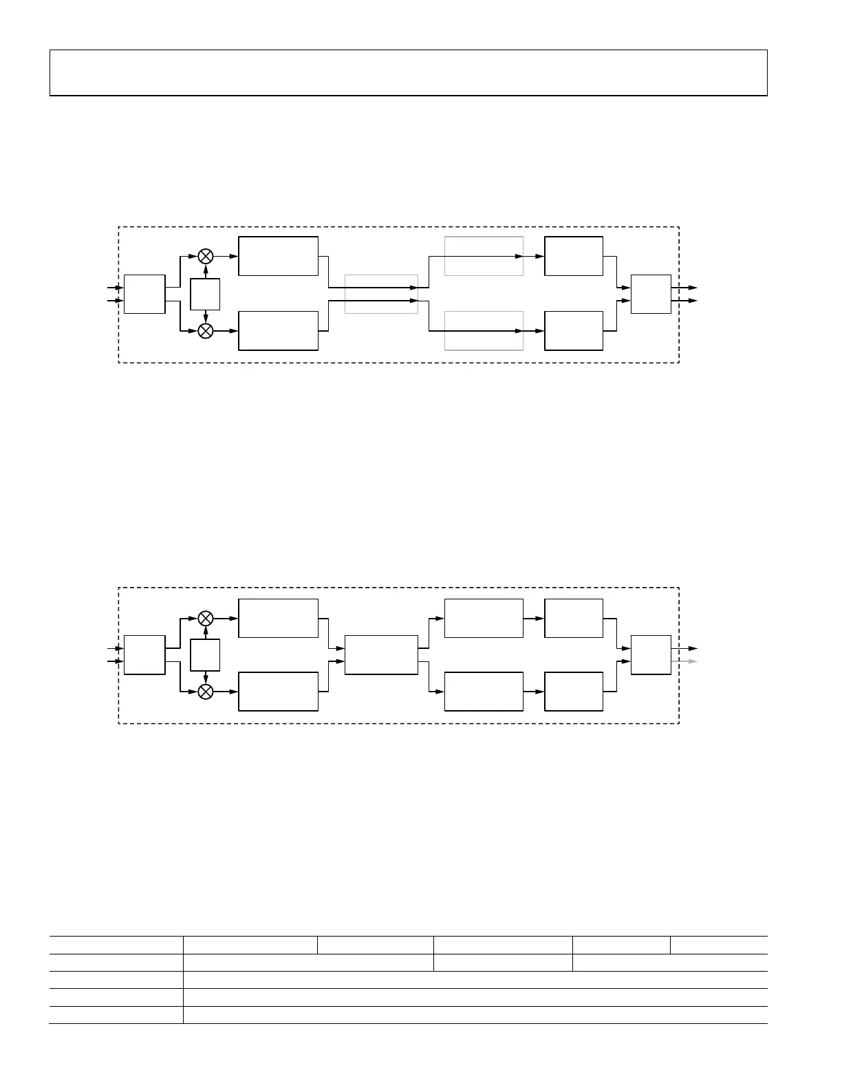
DPD Rx Function Name Description
adi_adrv9001_dpd_Initial_Configure
Configures the pre initial calibration DPD parameters. Called by
adi_adrv9001_Utilities_InitRadio_Load() as part of device initialization.
adi_adrv9001_dpd_Initial_Inspect Inspects the pre initial calibration DPD parameters.
adi_adrv9001_dpd_Configure Configures the post initial calibration DPD parameters.
adi_adrv9001_dpd_Inspect Inspects the post initial calibration DPD parameters.
DPD TUNING AND TESTING
Figure 181 describes an example setup for testing the integrated DPD with the ADRV9001 evaluation board in narrowband applications.
(In narrowband applications such as TETRA, power amplifier input should be connected to the TX1 output and power amplifier output
should be connected to RX1B.) As shown in Figure 181, an LPF is required at the Tx1 output port to filter out the Tx harmonics before
feeding the signal to power amplifier driver (If the power amplifier driver has an internal LPF, then the external LPF is not needed). Since
the device uses square wave mixer, it produces strong odd-order harmonics. Without filtering those harmonics, the DPD performance
could be impacted. The step attenuators external to the ADRV9001 evaluation board are optional. Note it is important to set up the
external loopback path before operating the integrated DPD. To achieve optimal DPD performance for TETRA waveforms, it is
recommended to use an external LO source for transmitter due to possible better phase noise performance, while the receiver LO
remains internal because the RF receive signal is downconverted to an IF instead of directly to baseband. For wideband applications, the
setup is similar but both transmitter and receiver LOs could be set to be internal because a wideband signal is less sensitive to phase
noise. A spectrum analyzer can be set up to observe the ACPR performance during a DPD operation.
XILINX
ZYNQ
FPGA BOARD
SIGNAL
GENERATOR
PC
POWER
AMPLIFIER
AMPLIFIER
DRIVER
FOR CAPTURING SPECTRUM ANALYZER SCREEN SHOT
GPIB
POWER
DIVIDER/
DIRECTIONAL
COUPLER
Tx1 PORT
Rx1 PORT
STEP
ATTENUATOR
HIGH POWER
ATTENUATOR
USB TO
ETHERNET
ADAPTER
USB TO
GPIB
ADAPTER
SPECTRUM
ANALYZER
ETHERNET
USB
USB
REFERENCE
CLOCK
POWER
DIVIDER
Tx EXTERNAL LO1
EXTERNAL
REFERENCE
CLOCK
EXTERNAL
REFERENCE
CLOCK
LPF
ADRV9001
TES
ADRV9001
EVAL
BOARD
24159-154
Figure 182. An Example Setup for Testing the Integrated DPD in Narrowband Applications
Once the setup is ready, user should further configure the TES and available external components properly which includes the following
major steps:
• Select desired profile.
• Perform board configuration to indicate external loopback path with external power amplifier is available.
• Enter the peak power of the loopback signal (ideally, it should be adjusted to be -18dBm±5dB. This could be achieved by tuning the
external step attenuator).
• Measure the external loopback delay and provide it through TES. This could be done through API commands which will be
discussed at the end of this section.
• Configure other initialization parameters such as RF frequency, LO source, and so on as desired. Also, enabling DPD for transmitter
and configure the model tap polynomial terms. It is recommended to start with the default model tap. (The method of tuning the
model tap order will be discussed in the next section.)
• Turn on DPD tracking calibration and all the other available tracking calibrations and start with the default DPD post calibration
parameter settings provided in TES.
• After programming, load, and play the provided sample transmit input file.
 Loading...