Preliminary Technical Data UG-1828
Rev. PrB | Page 193 of 277
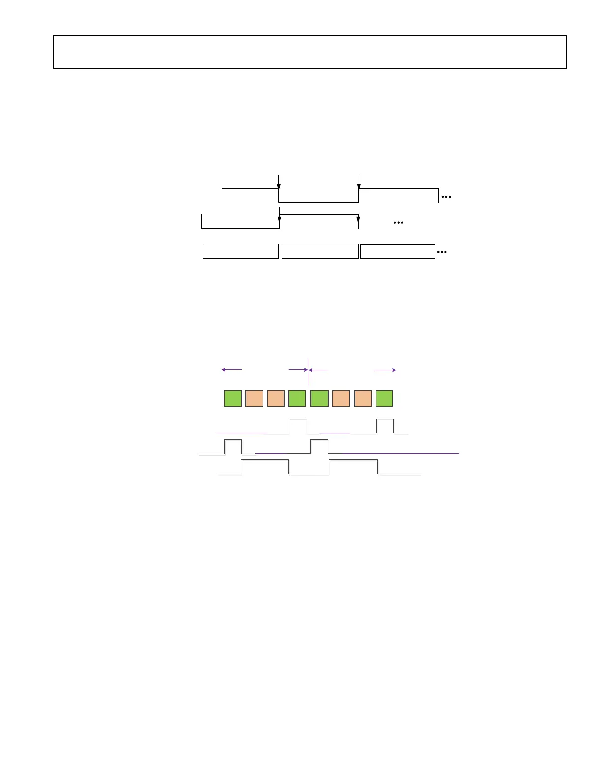
are assigned “increment attenuation” or “decrement attenuation” functionality. By applying a high pulse on the assigned GPIO pin, the
attenuation for a specific channel is either increased or decreased, depending on the assigned functionality. The pulse width requirement
is 2 system clock cycles (184.32 MHz) in the logic high state. Increment and decrement functionality can be assigned to any digital GPIO
from DGPIO_0 to DGPIO_15. Pin-based Tx attenuation control allows multiple increments or decrements of Tx attenuation.
Set Tx attenuation control mode to “GPIO_MODE” by the API function adi_adrv9001_Tx_Attenuation_Configure() or
adi_adrv9001_Tx_AttenuationMode_Set(), and select the properly GPIOs for each channel by the API function
adi_adrv9001_Tx_Attenuation_PinControl_Configure(), baseband processor can send the pulses to ADRV9001 via the specific digital
GPIO pins to increase or decrease the Tx attenuation.
Pin-Based Rx Gain Control
A complete description of Rx Gain control is provided in the Transmitter Signal Chain section of this User Guide.
Pin-based Rx gain control is relevant for applications which require Manual Gain Control (MGC) and precise timing for gain change
events. The pin-based control offers lower latency than SPI based gain change operations. In pin-based gain control, certain digital GPIO
pins are assigned “increment gain index” or “decrement gain index” functionality for a particular receiver channel. By applying a high
pulse on the assigned GPIO pin, the gain index for a specific channel is either increased or decreased, depending on the assigned
functionality. The pulse width requirement is 2 AGC clock cycles (184.32 MHz) in the logic high state. Increment and decrement
functionality can be assigned to any digital GPIO from DGPIO_0 to DGPIO_15.
Note that if the user has programmed a gain table that operates in a subset of the full gain table range (i.e. using index 195 to 255), once
the gain Index has reached Min/Max Gain index subsequent the pin-based Rx gain control rising edge will not change the gain index.
Set Rx Gain control mode to “PIN” by the API function adi_adrv9001_Rx_GainControl_Configure() or
adi_adrv9001_Rx_GainControl_Mode_Set(), configures the properly digital GPIO pins for gain increase and decrease control and other
control parameters by API function adi_adrv9001_Rx_GainControl_PinMode_Configure(), then baseband processor can send the
pulses to ADRV9001 via the specific digital GPIO pins to increase or decrease the Rx Gain index.
Power Amplifier Ramp Control
A complete description of power amplifier ramp control is being provided in the user guide in the future.
When the power amplifier ramp control function is used in ADRV9001, certain digital GPIO pin can be assigned as the “power amplifier
ramp control enable” functionality driven by the baseband processor, the rising edge of power amplifier ramp control enable with
programable delay will be act as the ramp up trigger signal and the falling edge of power amplifier ramp enable with programable delay
acts as the ramp down trigger signal.
Monitor Enable
See the Power Saving and Monitor Mode section for a complete description of monitor mode.
When the monitor mode is initialized in ADRV9001, certain digital GPIO is assigned as “Mon_enable” functionality driven by the
baseband processor, after necessary parameters initialization for monitor mode, by de-asserting and asserting the monitor enable pin will
enable the transitions between the Normal and Monitor operation modes or wake up ADRV9001 from sleep state at the falling edge of
“Mon_enable”.
Hopping Mode Control
TBD.
Digital GPIO Output Features
This section outlines digital GPIO output features available on the device. Output GPIO features on ADRV9001 use a concept called
source control. The source control describes what is the source of the signals routed to GPIO pins, whether they are from the monitor
feature or the ARM.
 Loading...