Preliminary Technical Data UG-1828
Rev. PrB | Page 151 of 277
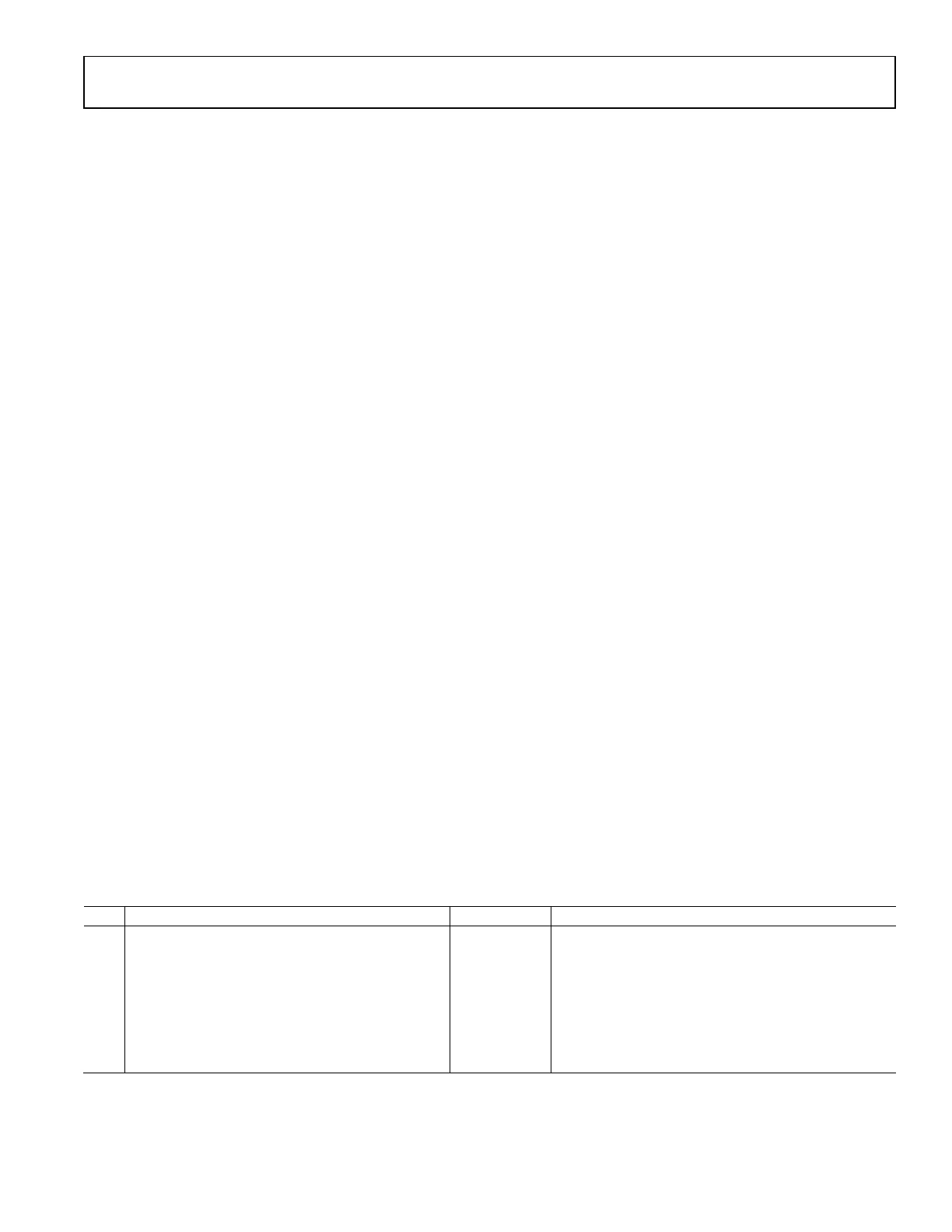
Figure 144 describes a high level flow chart of Rx gain control programming. Note the final step is to configure any GPIOs as necessary
such as GPIO inputs which allow the AGC gain update counter to be synchronized to a slot boundary, or DGPIOs to directly control the
gain index. Note the configure of the DGPIO pins for retrieving signal detectors information is included in the API command
adi_adrv9001_Rx_GainControl_Configure(). The operation of these has been described earlier.
GAIN CONTROL
SETUP START
CONFIGURE GAIN TABLE,
AGC STRUCTURES
RUN
adi_adrv9001_Rx_GainControl_Configure( )
RUN
adi_adrv9001_Rx_GainControl_Mode_Set( )
CONFIGURE GAIN
CONTROL GPIOS
GAIN CONTROL SETUP
COMPLETE
24159-118
Figure 145. Gain Control Programming Flowchart
Gain Control Data Structures
Figure 145 shows the member structure of adi_adrv9001_GainControlCfg_t, and its substructures, adi_adrv9001_PeakDetector_t,
adi_adrv9001_PowerDetector_t and adi_adrv9001_ExtLna_t. Each of the parameters are briefly explained in Table 67 to Table 70 the wider
context of these parameter settings being outlined in the previous relevant sections.