Preliminary Technical Data UG-1828
Rev. PrB | Page 205 of 277
Careful design of the dc bias network is required to ensure optimal RF performance levels. When designing the dc bias network, select
components with low dc resistance (R
DCR
) to minimize the voltage drop across the series parasitic resistance element with either of the
suggested dc bias schemes suggested in Figure 195. The R
DCR
resistors indicate the parasitic elements. As the impedance of the parasitics
increase, the voltage drop (ΔV) across the parasitic element increases causing the transmitter RF performance (that is, PO 1 dB PO MAX,
and so forth) to degrade. The choke inductance (LC) should be selected high enough relative to the load impedance such that it does not
degrade the output power.
The recommended dc bias network is shown in Figure 196. This network has fewer parasitic and fewer total components.
V
DC
= 1.8V
C
B
R
DCR
ΔV
V
BIAS =
1.8V – ΔV
V
BIAS =
1.8V – ΔV
ΔV
R
DCR
L
C
+
–
+
–
L
C
OUTPUT
STAGE
I
BIAS
= ~100mA
Tx1–/Tx2–
Tx1+/Tx2+
24159-168
I
BIAS
= ~100mA
Figure 196. ADRV9001 RF DC Bias Configurations Depicting Parasitic Losses Due to Wire Wound Chokes
ΔV
V
BIAS =
1.8V – ΔV
V
BIAS =
1.8V – ΔV
+–
ΔV
+–
C
B
Tx1 OR Tx2
OUTPUT
STAGE
I
BIAS
= ~100mA
1.8V
R
DCR
R
DCR
I
BIAS
= ~100mA
Tx1–/Tx2–
Tx1+/Tx2+
Figure 197. ADRV9001 RF DC Bias Configurations Depicting Parasitic Losses Due to Center Tapped Transformers
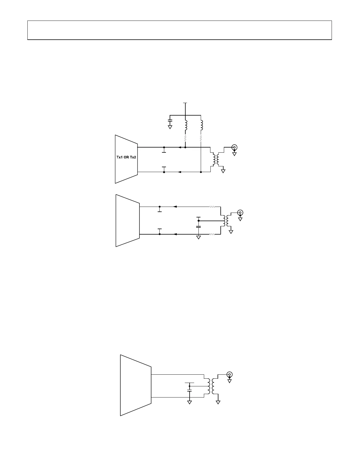
Figure 197 to Figure 200 identify four basic differential transmitter output configurations. Impedance matching networks (balun single-
ended port) are most likely to be required to achieve optimum device performance from ADRV9001. Also, the transmitter outputs must
be ac-coupled in most applications due to the dc bias voltage applied to the differential output lines of the transmitter.
The recommended RF transmitter interface is shown in Figure 197 featuring a center tapped balun. This configuration offers the lowest
component count of the options presented.
Brief descriptions of the transmitter port interface schemes are provided as follows.
• Center tapped transformer passes the bias voltage directly to the transmitter outputs
• RF chokes are used to bias the differential transmitter output lines. Additional coupling capacitors (CC) are added in the creation of
a transmission line balun
• RF chokes are used to bias the differential transmitter output lines and connect into a transformer
• RF chokes are used to bias the differential output lines that are ac-coupled into the input of a driver amplifier
Transmitter Interface Configurations
Tx1 OR Tx2
OUTPUT STAGE
1.8V
C
B
24159-170
Tx1–/Tx2–
Tx1+/Tx2+
Figure 198. ADRV9001 RF Transmitter Interface Configuration A
 Loading...