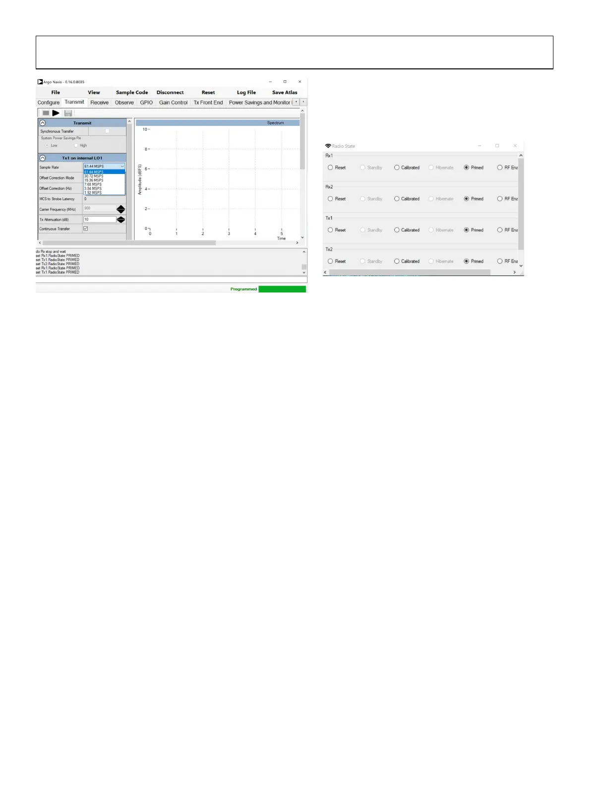
UG-1828 Preliminary Technical Data
Rev. PrB | Page 220 of 277
0
5.0
–5.0
2.0
1.0
–1.0
–2.0
0.5
–0.5
0.2
–0.2
m1
FREQUENCY = 10.00MHz
S(5,5) = 0.997/–402
IMPEDANCE = 9.694E3 + j2.467E4
m2
FREQUENCY = 100.0MHz
S(5,5) = 0.997/–4.067
IMPEDANCE = 137.890 – j2.809E3
m3
FREQUENCY = 300.0MHz
S(5,5) = 0.990/–12.133
IMPEDANCE = 46.714 – j938.620
m4
FREQUENCY = 600.0MHz
S(5,5) = 0.969/–23.831
IMPEDANCE = 36.427 – j471.206
m5
FREQUENCY = 1.000GHz
S(5,5) = 0.932/–38.422
IMPEDANCE = 32.096 – j283.752
FREQUENCY (100.0kHz TO 1.000GHz)
S(5,5)
M5
M3
M2
M1
M4
24159-189
Figure 217. Device Clock Input Series Equivalent Differential Impedance
Device clock input board traces connected to device clock inputs balls should be implemented with stripline transmission lines using
inner copper layers in PCB stackup. The frequency of device clock input signal can go as high as 1GHz and stripline transmission line
approach will provide better signal integrity of clock signal especially at higher frequency as well as superior shielding of RF emission of
device clock signal.
The DEV_CLK_IN signal is available on the DEV_CLK_OUT pin. Table 97 describes default division applied to DEV_CLK_IN signal
after power up. Use can change this divider later on using API command. It should be noted that DEV_CLK_OUT pin is a CMOS type
pin. It is intended to be used to provide clock to BBIC or on-board microcontroller or audio CODEC type devices. It is not intended to
be used by another RF sensitive IC.
DEV_CLK_IN PHASE NOISE REQUIREMENTS
To prevent performance degradation, the DEV_CLK reference must be a very clean signal. Best performance from the synthesizer would
result if the applied reference were ideal, however that is unrealistic. Table 98 lists the required phase noise of the DEV_CLK signal for a
1dB system PN degradation compared to an ideal DEVICE CLOCK. For different DEV_CLK frequencies, the table can be scaled
appropriately. Clock source with phase noise performance outlined in Table 98 (or better) allows ADRV9001 to deliver datasheet
performance. It should be noted that Table 98 provide reference information for ADRV9001 operating with LTE type standards. Each
standard will determine its own DEV_CLK phase noise requirements. As an example, Table 99 provides recommendation for DEV_CLK
when ADRV9001 is intended to operate with LMR type standards. Ideally DEV_CLK phase noise requirement should be derived from
customer specific application and its requirements set for adjacent channel rejection.
In general, using a higher phase noise source can degrade performance delivered by ADRV9001 transceiver.
Table 98. DEV_CLK_IN Phase Noise Requirements for 1dB system PN degradation compared to an ideal DEVICE CLOCK
Frequency Offset
From Carrier
Narrow PLL Loop Bandwidth (Approximately
50 kHz) (Default, Typically <3 GHz)
Wide PLL Loop Bandwidth (Approximately 300 kHz)
(User Configured, Typically >3 GHz )
122.88 MHz
(dBc/Hz)
153.6 MHz
(dBc/Hz)
245.76 MHz
(dBc/Hz)
122.88 MHz
(dBc/Hz)
153.6 MHz
(dBc/Hz)
245.76 MHz
(dBc/Hz)
100 Hz −113.02 −111.08 −107.00 −114.02 −112.08 −108.00
1000 Hz −125.02 −123.08 −119.00 −127.02 −125.08 −121.00
10 kHz −133.02 −131.08 −127.00 −138.02 −136.08 −132.00
100 kHz −137.02 −135.08 −131.00 −146.02 −144.08 −140.00
1 MHz −133.02 −131.08 −127.00 −147.02 −145.08 −141.00
10 MHz −104.02 −102.08 −98.00 −118.02 −116.08 −112.00
 Loading...