Preliminary Technical Data UG-1828
Rev. PrB | Page 231 of 277
Balanced lines for differential mode signalling used between the device and the RF balun should be as short as possible. The length of the
single ended transmissions lines for RF signals should also be as short as possible. Keeping signal paths as short as possible reduce
susceptibility to undesired signal coupling and reduce the effects of parasitic capacitance, inductance, and loss on the transfer function of
the transmission line and impedance matching network system. The routing of these signal paths is the most critical factor in optimizing
performance and, therefore, should be routed prior to any other signals and maintain the highest priority in the PCB layout process.
BOTTOM SIDE
ALTERNATIVE,
LOWER-BANDS
BALUN FOOTPRINT
HIGHER-BANDS BALUN
FOOTPRINT
SINGLE-ENDED PI
NETWORK
RESISTOR/OPTIONAL AC
COUPLING CAPACITOR
SWITCHING NETWORK
DIFFERENTIAL
PI NETWORK
TOP SIDE
24159-198
Figure 227. Receiver Matching Network on ADRV9001 Evaluation Board
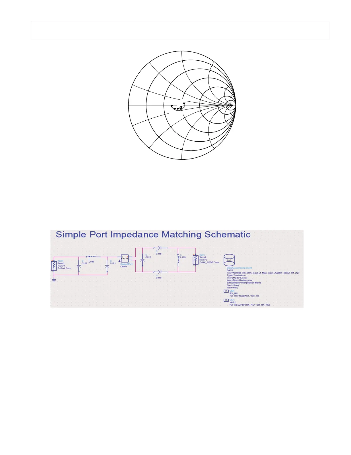
The circuit in Figure 226 shows the layout topology for the chosen receiver matching network. Note the location and orientation of each
component – placement is critical to achieve expected performance. Similarly, the circuit in Figure 227 shows the layout topology used
for the transmitter matching network. (see the RF Port Interface Information section for circuit details). More details concerning the dc
supply to the transmitter section are provided in the next section.
All the RF signals must have a solid ground reference under each path to maintain the desired impedance. None of the critical traces
should run over a discontinuity in the ground reference.
 Loading...