Preliminary Technical Data UG-1828
Rev. PrB | Page 235 of 277
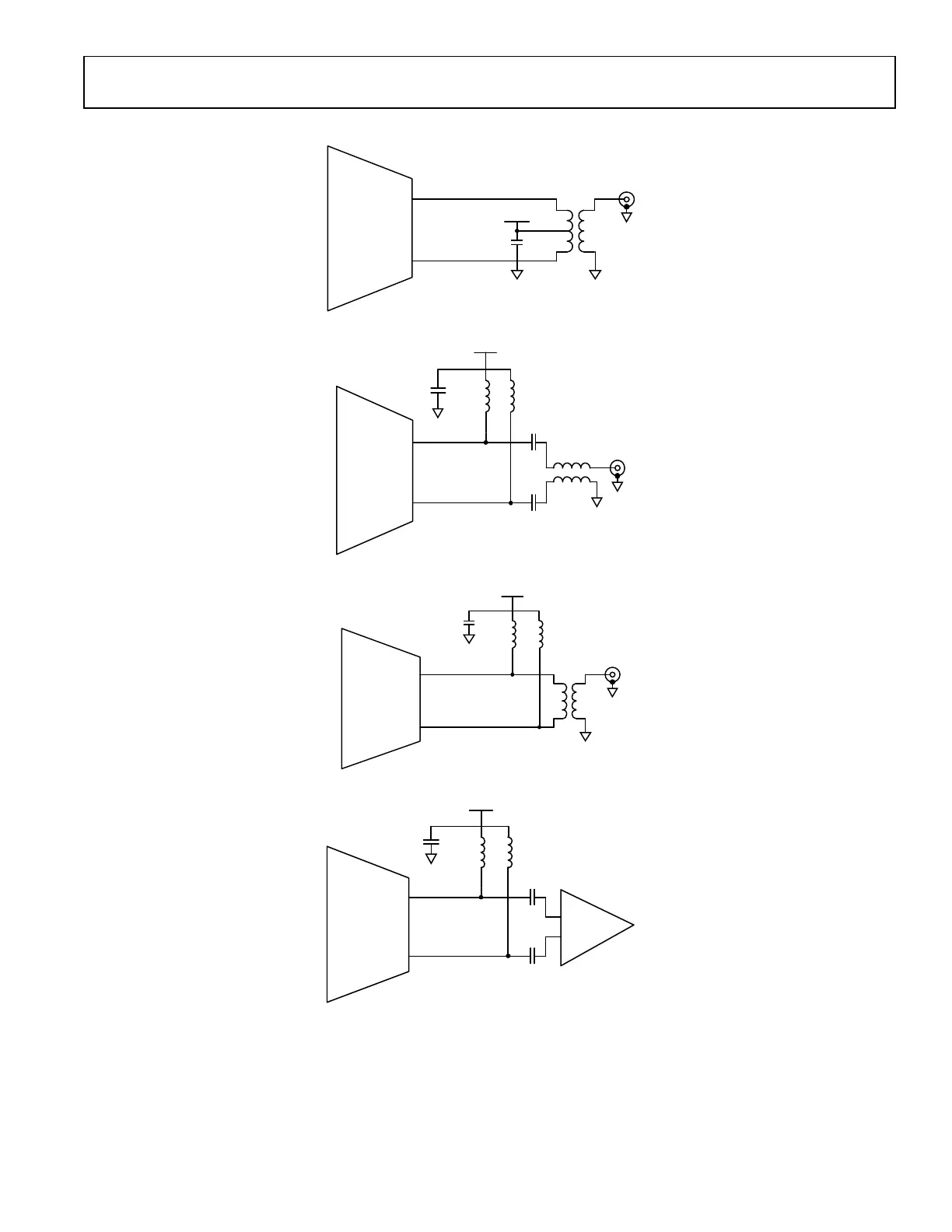
SERIES MATCHING
COMPONENTS
DECOUPLING
CA
PACI
TORS
Tx DC POWER
FEED CHOKES
BALUN
RF BALUN SELECTION AND
DIFFERENTIAL/SINGLE-ENDED SERIES
DC BLOCKING COMPONENTS
DC FEED FROM
VANA1/2_1P8 PLANE
24159-201
Figure 233. Transmitter Power Supply Using RF Chokes
SSI Data Port Trace Routing Recommendations
The Data Port interface transfer I/Q data between BBIC/FPGA and ADRV9001 Tx and Rx datapaths. There are two possible mode of
operation for SSI data port:
• CMOS-SSI mode – single ended - with clock rate for data transfer up to 80 MHz
• LVDS-SSI mode – differential - with clock rate for data transfer up to 500 MHz DDR (1000 MHz data rate)
Correct layout practice should be followed while routing SSI interface signals.
If CMOS-SSI mode is selected, single-ended signal lines between ADRV9001 and BBIC/FPGA should be as short as possible. Trace
capacitance should also be minimized to minimize the current needed by ADRV9001 to drive the line. Refer to the ADRV9001 datasheet
document for details regarding pin drive capabilities.
If LVDS-SSI mode is selected, the user should route all LVDS signals as 100 Ω differential pairs.
• When routing the PCB layout for LVDS-SSI data lines, the designer must decide to route the signals using stripline or microstrip
traces. There are positives and negatives for each that should be carefully considered.
• Stripline has less loss and emits less EMI than microstrip lines, but stripline traces require the use of vias that can add complexity to
the task of controlling the impedance by adding line inductance.
Microstrip is easier to implement if the component placement and density allow for routing on the top layer, simplifying the task of
controlling the impedance.
If using the top layer of the PCB is problematic or the advantages of stripline are desirable, then follow these recommendations:
• Minimize the number of vias.
• Use blind vias wherever possible to eliminate via stub effects, and use micro-vias to minimize via inductance.
• If using standard vias, use maximum via length to minimize the stub size. For example, on an 8-layer board, use layer 7 for the
stripline pair.
• For each via pair, a pair of ground vias should be placed in close proximity to them to minimize the impedance discontinuity.
In LVDS-SSI mode
• for Tx data port inputs, termination of 100Ω is implemented inside ADRV9001
• for Rx data port outputs, it is expected that 100 Ω termination is implemented at the receiver end.
 Loading...