Handler Interface
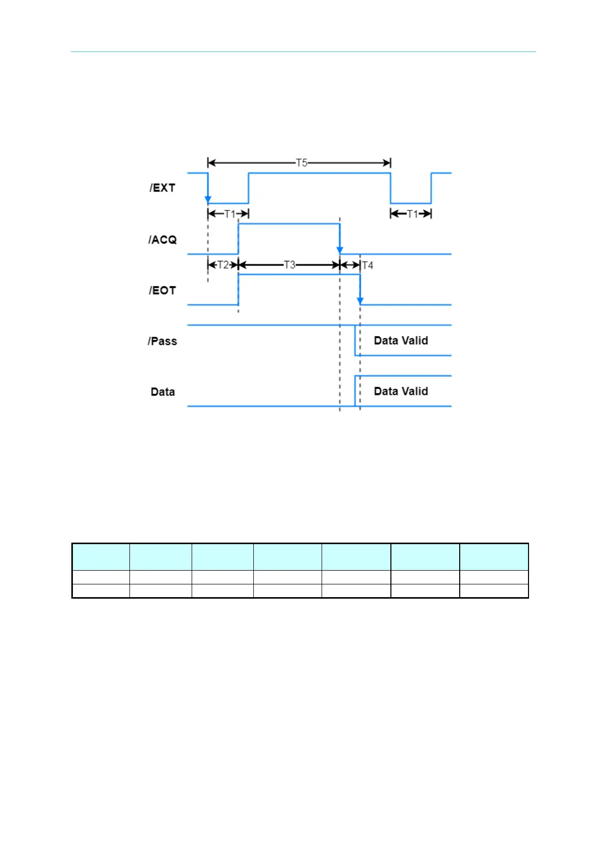
9.4 Pin Timing Diagram of Handler Interface
Test conditions: Test Voltage 1000V, C.C. 50mA, Hold Range 20mA, Charge Time 5ms, Dwell
Time 5ms, Integration Time 1ms
Descriptions for various signals are as the following:
T1: Pulse width of trigger signal
T2: Measurement delay time
T3: Required time for measuring an entry of test value
T4: Data transfer time
T5: Measurement the shortest interval time between two entries of test values
Data: It includes judgment signals of /FAIL, /C_CHK FAIL, /PD_Fail, /HI, /LO,
/FAIL_CHG_DISCHG, etc.