GR740-UM-DS, Nov 2017, Version 1.7 440 www.cobham.com/gaisler
GR740
The recommended power sequence when powering up the device is as below. Between each step there
can be an arbitrary amount of delay.
1. The sys_resetn signal must be controlled to a low logic level, and remain at logic low through the
sequence up to step 7. Other signals should be within recommended operating conditions.
2. Raise the two I/O voltage rails VIO3V3 and VIO2V5, in arbitrary order, up to nominal voltage
3. Static configuration signals, such as pll_bypass should be controlled to their intended levels at this
point.
4. Raise the core and PLL digital supplies VDD12 and VDDPLLD up to their nominal voltage.
5. If necessary, wait until input clocks to the system (SYS_CLK, MEM_EXTCLK, SPW_CLK) are
stable. (unused clock inputs should be at constant low or constant high level)
6. Raise the PLL analog supply VDDPLLA up to its nominal voltage
7. Wait for a minimum time of t
PLL0
and then raise the sys_resetn input signal
39.4.2 Power-down sequence
This section is provided as a design guideline.
One of the below two means of power-down are recommended:
Natural power-down - stopping the supply of current to all power rails on board level simultaneously
and then letting the capacitances of the supply rails discharge at their natural rate. The I/Os should
remain within the recommended operating conditions (in other words decrease as the I/O supply falls)
Sequenced power-down - Dropping the voltages one by one in reverse order of the power-up
sequence.
39.4.3 Cold sparing support
While all supply rails to the device are powered down, normal I/O level voltages may be present on
the device I/O pins without causing any inrush current into the device. The device will draw some
minor leakage current (limited by I
leak
). Before starting the power-up sequence described above on a
device that has been acting as cold spare, all (to become) outputs should have returned to an undriven
state.
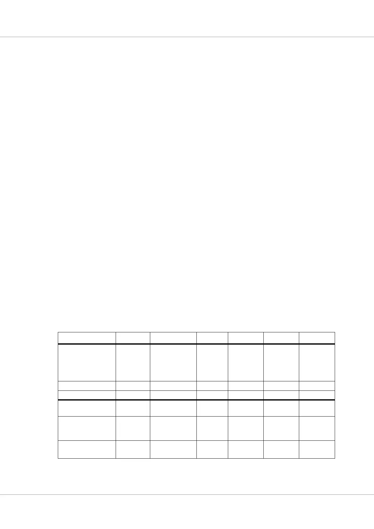
Table 577.Recommended DC operating conditions and characteristics for device acting as cold spare
Parameter Symbol Conditions Minimum Typical Maximum Unit
Supply voltage VDD12,
VDIG25,
VDIG33,
VDDPLLA,
VDDPLLD
0.000 0.000 V
I/O level, LVCMOS -0.300 3.600 V
I/O level, LVDS pins 0.000 2.000 V
I/O leakage current
(LVCMOS)
I
leak,LVCMOS
-0.010 0.010 mA
I/O leakage current
(LVDS)
I
leak,LVCMOS
Not counting cur-
rent on inputs dur
to R
I,LVDS
015mA
LVDS input resis-
tance
2)
R
I,LVDS
80 100 120 Ohm