GR740-UM-DS, Nov 2017, Version 1.7 101 www.cobham.com/gaisler
GR740
10.4 SDRAM back-end operation
10.4.1 General
Synchronous dynamic RAM (SDRAM) access is supported to 1-4 external banks of PC100 compati-
ble devices. Each external bank has a separate chip select signal mapped to pins according to table 85.
The controller supports devices with 8 - 12 column-address bits, up to 13 row-address bits, and 4
internal banks. The size of each of the external banks can be programmed in binary steps between 4
Mbyte and 512 Mbyte in half-width mode, and between 8 Mbyte and 1 Gbyte in full-width mode. The
operation of the SDRAM controller is controlled through the configuration register SDCFG (see sec-
tion 10.6).
10.4.2 Initialization
When the SDRAM controller is enabled, it automatically performs the SDRAM initialization
sequence of PRECHARGE, 8x AUTO-REFRESH and LOAD-MODE-REG on both banks simultane-
ously. The controller programs the SDRAM to use page burst on read accesses and single location
access on write accesses.
10.4.3 Read and write cycles
A read cycle is started by performing an ACTIVATE command to the desired bank and row, followed
by a READ command with data read after the programmed CAS delay. The read cycle is terminated
with a PRE-CHARGE command, no banks are left open between two accesses.
Write cycles are performed similarly to read cycles, with the difference that WRITE commands are
issued after activation.
10.4.4 Configurable SDRAM timing parameters
To provide optimum access cycles for different SDRAM devices (and at different frequencies), three
SDRAM parameters can be programmed through the memory configuration register (SDCFG):
TCAS, TRP and TRFCD. The value of these fields affect the SDRAM timing as described in table 83.
If the TCAS, TRP and TRFC are programmed such that the PC100 specifications are fulfilled, the
remaining SDRAM timing parameters will also be met. The table below shows typical settings for
100 MHz operation and the resulting SDRAM timing (in ns). Note that in addition to these settings,
the setup and hold timings must be satisfied to use the memory at a specific frequency.
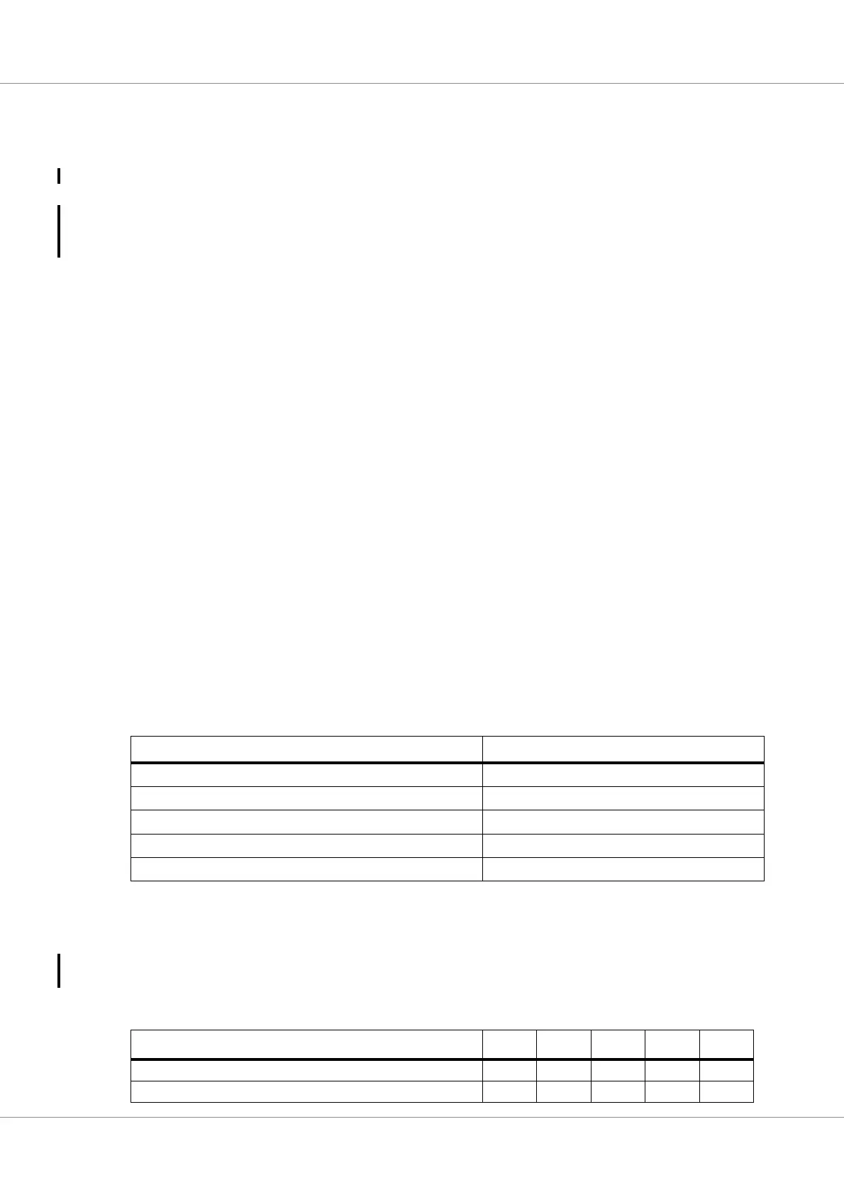
Table 83. SDRAM programmable minimum timing parameters
SDRAM timing parameter Minimum timing (clocks)
CAS latency, RAS/CAS delay (t
CAS
, t
RCD
)TCAS + 2
Precharge to activate (t
RP
)TRP + 2
Auto-refresh command period (t
RFC
) TRFC + 3
Activate to precharge (t
RAS
) TRFC + 1
Activate to Activate (t
RC
) TRP + TRFC + 4
Table 84. SDRAM example programming
SDRAM settings
t
CAS
t
RC
t
RP
t
RFC
t
RAS
100 MHz, CL=2; TRP=0, TCAS=0, TRFC=4 20 80 20 70 50
100 MHz, CL=3; TRP=0, TCAS=1, TRFC=4 30 80 20 70 50