GR740-UM-DS, Nov 2017, Version 1.7 102 www.cobham.com/gaisler
GR740
10.4.5 Refresh
The SDRAM controller contains a refresh function that periodically issues an AUTO-REFRESH
command to both SDRAM banks. The period between the commands (in clock periods) is pro-
grammed in the refresh counter reload field in the SDCFG register. Depending on SDRAM type, the
required period is typically 7.8 or 15.6 s (corresponding to 780 or 1560 clocks at 100 MHz). The
generated refresh period is calculated as (reload value+1)/(memory clock period). The refresh func-
tion is enabled by setting bit 31 in the SDCFG register.
10.4.6 2T signaling mode
An alternative mode is supported in the controller where all address and control signals except for the
chip select is set for an extra cycle with chip select deasserted before the command is issued. This
improves the board timing analysis for these signals since an extra cycle of setup time is achieved.
The price of this is one extra SDRAM cycle of latency for the ACTIVATE command, resulting in one
cycle extra read latency, and also one extra cycle for the REFRESH. Also due to internal design rea-
sons, one extra cycle before PRECHARGE after a read burst (but not after writing) is also inserted,
however this does not affect latency as it is done in parallel with the transfer of read data to the AHB
domain.
The 2T signaling mode is activated by setting the EN2T bit in the SDRAM configuration register 2
SDCFG2) register.
In order for the 2T signaling mode to work, the mode register needs to be programmed for length-2
read and length-2 write bursts. Therefore, after changing the EN2T setting, the LOAD-MODE-REG-
ISTER command must be reissued by writing to the SDRAM command configuration register field
before proceeding with additional accesses.
10.4.7 Double chip select mode
As the 2T signaling mode improves analog setup time for all control signals except chip select, an
additional setting exists to group the four chip select outputs into two chip selects, where each chip
select signal is driven identically on two outputs in parallel. On the board, the two copies can each
then be routed to half of the SDRAM devices and thereby reduce the capacitive load on each output.
10.4.8 SDRAM commands
The controller can issue four SDRAM commands by writing to the SDRAM command field in the
SDRAM Configuration register: PRE-CHARGE, AUTO-REFRESH and LOAD-MODE-REG
(LMR). The command field will be cleared after a command has been executed. Note that when
changing the value of the CAS delay or enabling/disabling 2T signaling, a LOAD-MODE-REGIS-
TER command should be generated at the same time to update the mode register. The mode register is
programmed as shown in table 86.
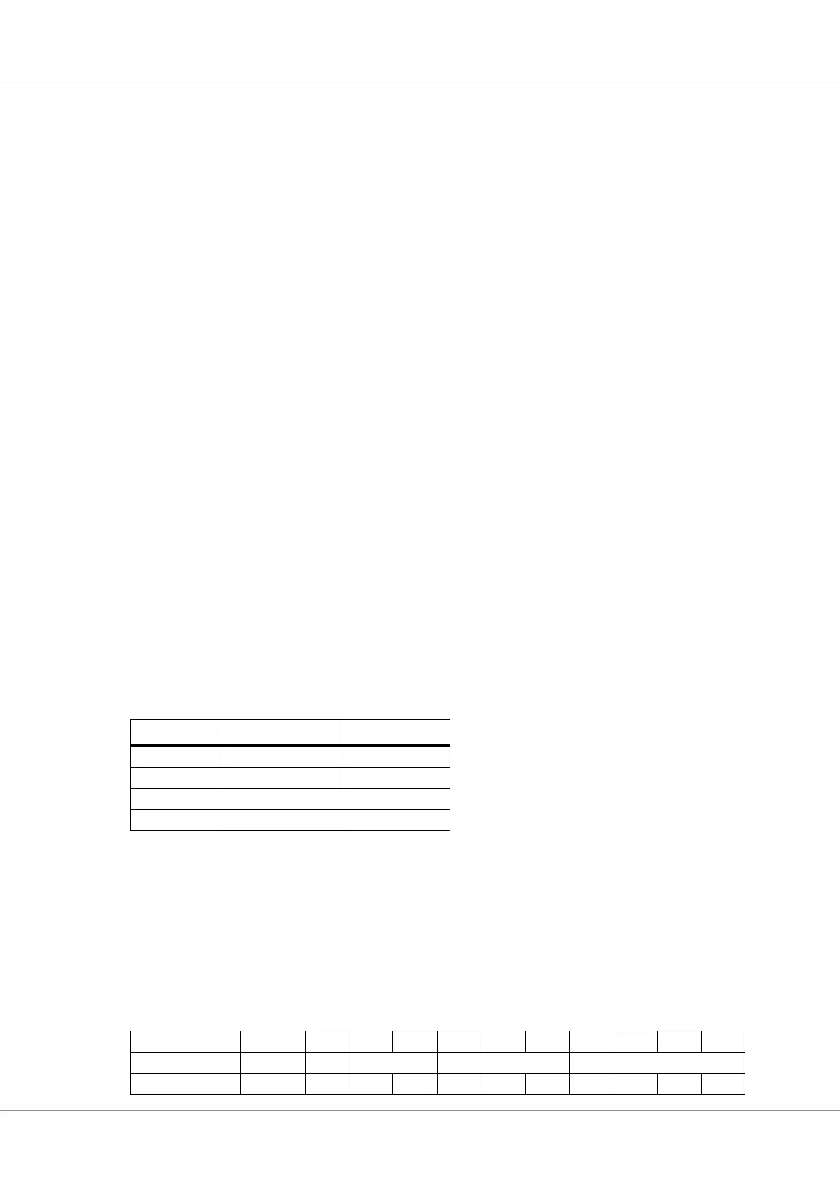
Table 85. Mapping of chip selects to I/Os
Pin Function DCS=0 Function DCS=1
mem_sn(0) CS(0) CS(0)
mem_sn(1) CS(1) CS(0)
mem_addr(13) CS(2) CS(1)
mem_addr(14) CS(3) CS(1)
Table 86. SDRAM controller mode register programming
Mode register bit12 .. 109876543210
(reserved) WB Op Mode CAS Latency BT Burst length
Controller setting0 EN2T0001CL000EN2T