EasyManuals Logo

CYG PRS-7367 User Manual

CYG PRS-7367
360 pages
To Next Page IconTo Next Page
To Previous Page IconTo Previous Page
Page #139 background imageLoading...
Page #139 background image
Protection Functions
PRS-7367 131
&
&
&
&
≥1
≥1
&
25SYN_T_DdChk / 0
Uref< 25SYN_Vol_DdANA
Usyn< 25SYN_Vol_DdANA
&
Uref> 25SYN_Vol_LvANA
Usyn< 25SYN_Vol_DdANA
&
Uref< 25SYN_Vol_DdANA
Usyn> 25SYN_Vol_LvANA
SIG VTS_ALm
SIG 25SYN_VTS_Usyn_ALm
SIG
25SYN_DdChk_Blk
SIG 25SYN_Blk
≥1
SIG25SYN_DdChk_OK
SIG25SYN_LL_DB_OK
SIG25SYN_DL_LB_OK
SIG25SYN_DL_DB_OK
25SYN_DL_DB SET
25SYN_DL_LB SET
25SYN_LL_DB SET
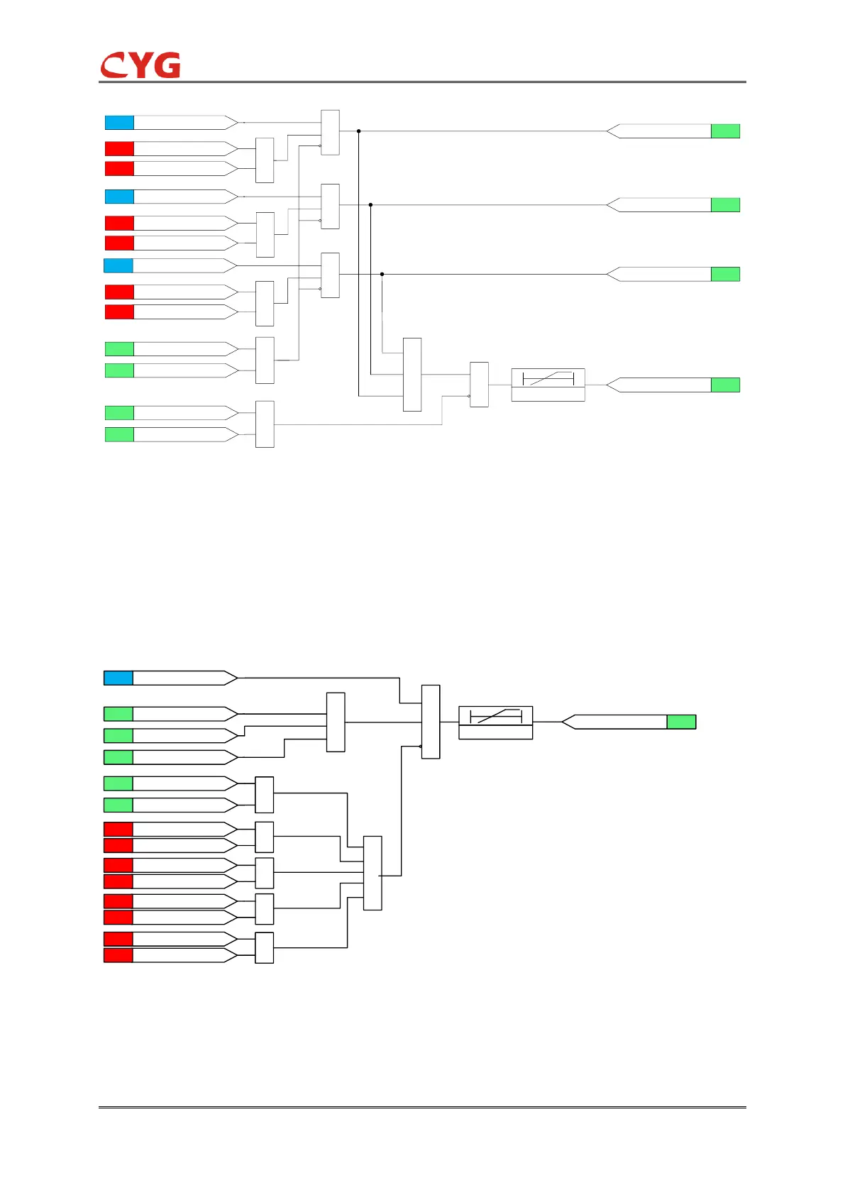
Figure 3.23-1 Logic Diagram of Dead charge check logic
The frequency difference, voltage difference, and phase difference of voltages from both sides of
the circuit breaker are calculated in the device, they are used as input conditions of the
synchronism check. When the synchronism check function is enabled and the voltages of both
ends meet the requirements of the voltage difference, phase difference, and frequency difference,
and there is no synchronism check blocking signal, and the measured bus voltage and line voltage
for synchro-check should not exceed the overvoltage threshold 25SYN_OV or lag the under
voltage threshold 25SYN_UV, it is regarded that the synchronism check conditions are met.
&
&
25SYN_T_SynChk / 0
SIG 25SYN_Vol_Diff_OK
SIG
25SYN_Fr_Diff_OK
SIG
25SYN_Ang_Diff_OK
SIG 25SYN_SynChk_Blk
SIG 25SYN_Blk
1
25SYN_SynSET
SIG25SYN_SynChk_OK
Uref> 25SYN_OVANA
Uref< 25SYN_UVANA
Usyn> 25SYN_OVANA
Usyn< 25SYN_UVANA
fref> 25SYN_OFANA
fref< 25SYN_UFANA
fsyn> 25SYN_OFANA
fsyn< 25SYN_UFANA
1
1
1
1
1
Figure 3.23-2 Logic Diagram of Synchronism check

Table of Contents

Questions and Answers:

Question and Answer IconNeed help?

Do you have a question about the CYG PRS-7367 and is the answer not in the manual?

CYG PRS-7367 Specifications

General IconGeneral
BrandCYG
ModelPRS-7367
CategoryControl Unit
LanguageEnglish