Protection Functions
146 PRS-7367
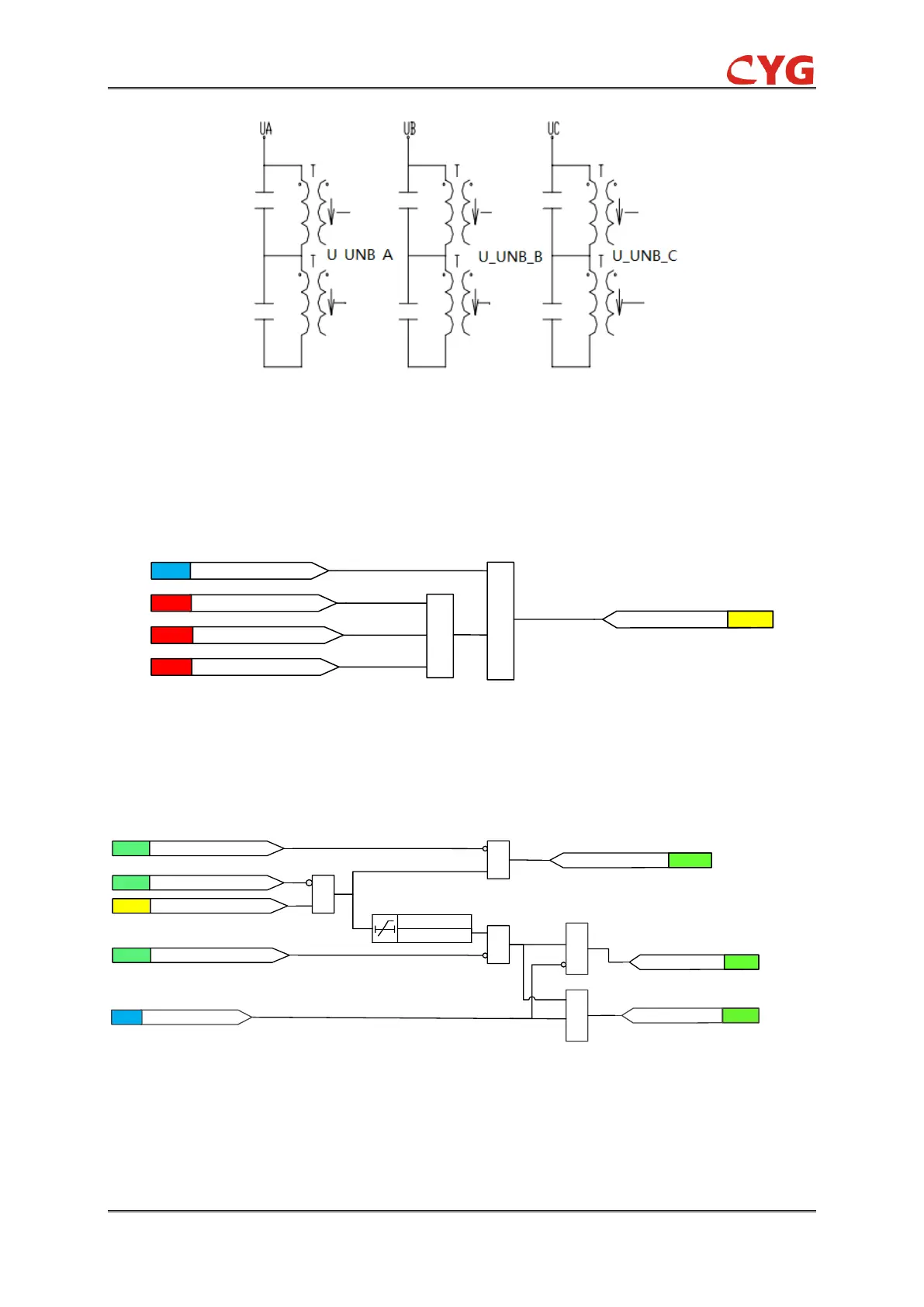
Figure 3.27-2 The three phase balance voltage of Y-connected capacitor bank
3.27.2.1 Initiation logic
The initiation of three phase voltage unbalance protection can be described by using a module
diagram. The functional module diagram is shown as below: the unbalance voltages U_UNB_A,
U_UNB_B and U_UNB_C are sampled in device by Ua2, Ub2, Uc2.
Initiation
FLG
Ua2 > 59NT_Vol_StrANA
Ub2 > 59NT_Vol_StrANA
Uc3 > 59NT_Vol_StrANA
SET
59NT_Ena=1
1
&
Figure 3.27-3 The initial diagram
3.27.2.2 Timer element
The functional module diagram is shown as below:
&
FLG
Initiation
59NT_STR
SIG
59NT_OP
SIG
SIG
59NT_BLK=1
SIG
59NT_BLK_ST=1
SIG
59NT_BLK_OP=1
&
&
30ms
59NT_Op_T
& 59NT_Alm
SIG
59NT_Alm_Ena=1
SET
&
Figure 3.27-4 Timer element
The time characteristic is according to DT. When the operation timer has reached the value set by
59NT_Op_T, the 59NT_Op output is activated. If the fault disappears before the module operates,
the operation will reset with a time delay of 30 ms.