Titanium Interfaces User Guide
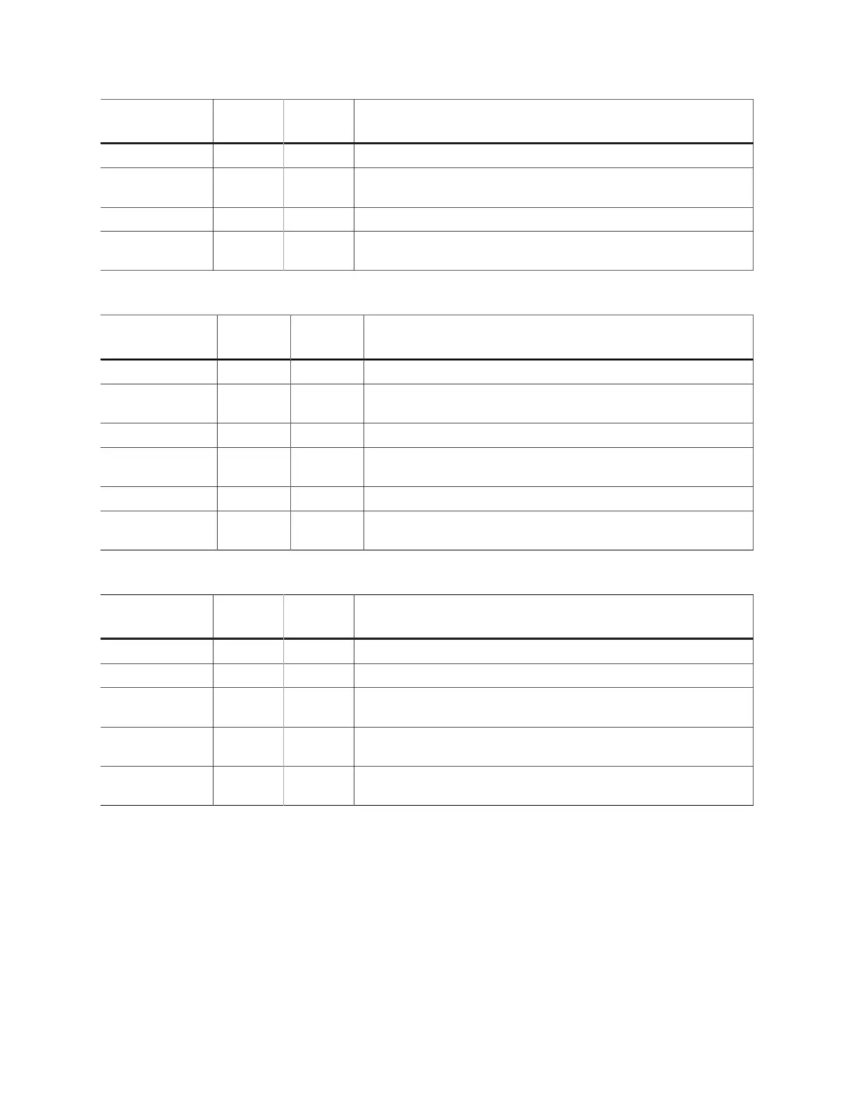
Table 16: AXI4 Write Response Channel Signals (Interface to FPGA Fabric)
Signal
x is 0 or 1
Direction Clock
Domain
Description
BID_x[5:0] Output ACLK_x Response ID tag. This signal is the ID tag of the write response.
BREADY_x Input ACLK_x Response ready. This signal indicates that the master can accept a
write response.
BRESP_x[1:0] Output ACLK_x Read response. This signal indicates the status of the read transfer.
BVALID_x Output ACLK_x Write response valid. This signal indicates that the channel is
signaling a valid write response.
Table 17: AXI4 Read Data Channel Signals (Interface to FPGA Fabric)
Signal
x is 0 or 1
Direction Clock
Domain
Description
RDATA_x[511:0] Output ACLK_x Read data.
RID_x[5:0] Output ACLK_x Read ID tag. This signal is the identification tag for the read data
group of signals generated by the slave.
RLAST_x Output ACLK_x Read last. This signal indicates the last transfer in a read burst.
RREADY_x Input ACLK_x Read ready. This signal indicates that the master can accept the
read data and response information.
RRESP_x[1:0] Output ACLK_x Read response. This signal indicates the status of the read transfer.
RVALID_x Output ACLK_x Read valid. This signal indicates that the channel is signaling the
required read data.
Table 18: AXI4 Write Data Channel Signals (Interface to FPGA Fabric)
Signal
x is 0 or 1
Direction Clock
Domain
Description
WDATA_1[511:0] Input ACLK_x Write data. AXI4 port 0 is 256, port 1 is 128.
WLAST_x Input ACLK_x Write last. This signal indicates the last transfer in a write burst.
WREADY_x Output ACLK_x Write ready. This signal indicates that the slave can accept the write
data.
WSTRB_x[63:0] Input ACLK_x Write strobes. This signal indicates which byte lanes hold valid data.
There is one write strobe bit for each eight bits of the write data bus.
WVALID_x Input ACLK_x Write valid. This signal indicates that valid write data and strobes are
available.
www.efinixinc.com 35