Titanium Interfaces User Guide
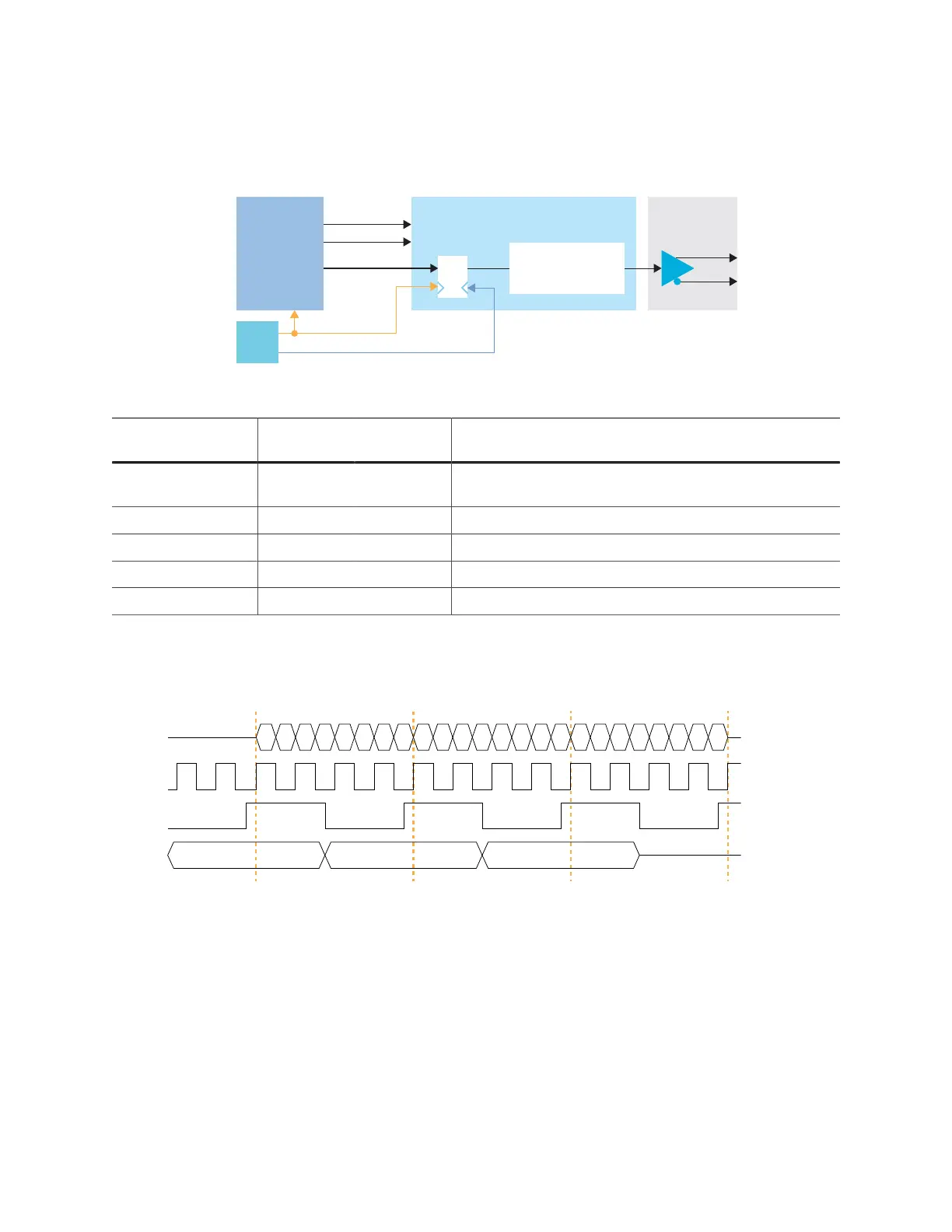
LVDS TX
You can configure an HSIO block as one LVDS TX signal. LVDS TX can be used in the
serial data output mode or reference clock output mode.
Figure 24: LVDS TX Interface Block Diagram
Table 39: LVDS TX Signals (Interface to FPGA Fabric)
Signal Direction Clock
Domain
Description
OUT[9:0] Input SLOWCLK Parallel output data from the core. The width is
programmable.
SLOWCLK Input – Parallel (slow) clock.
FASTCLK Input – Serial (fast) clock.
RST Input SLOWCLK (Optional) Resets the serializer.
OE Input – (Optional) Output enable signal.
The following waveform shows the relationship between the fast clock, slow clock, TX data
going to the pad, and byte-aligned data from the core.
Figure 25: LVDS Timing Example Serialization Width of 8 (Half Rate)
OUT is byte-aligned data passed from the core on the rising edge of SLOWCLK.
A
3
A
4
A
5
A
6
A
7
B
0
B
1
B
2
B
3
B
4
B
5
B
6
B
7
C
0
C
1
C
2
C
3
C
4
C
5
C
6
C
7
B[7:0] C[7:0]
www.efinixinc.com 70