Titanium Interfaces User Guide
LVDS Bidirectional
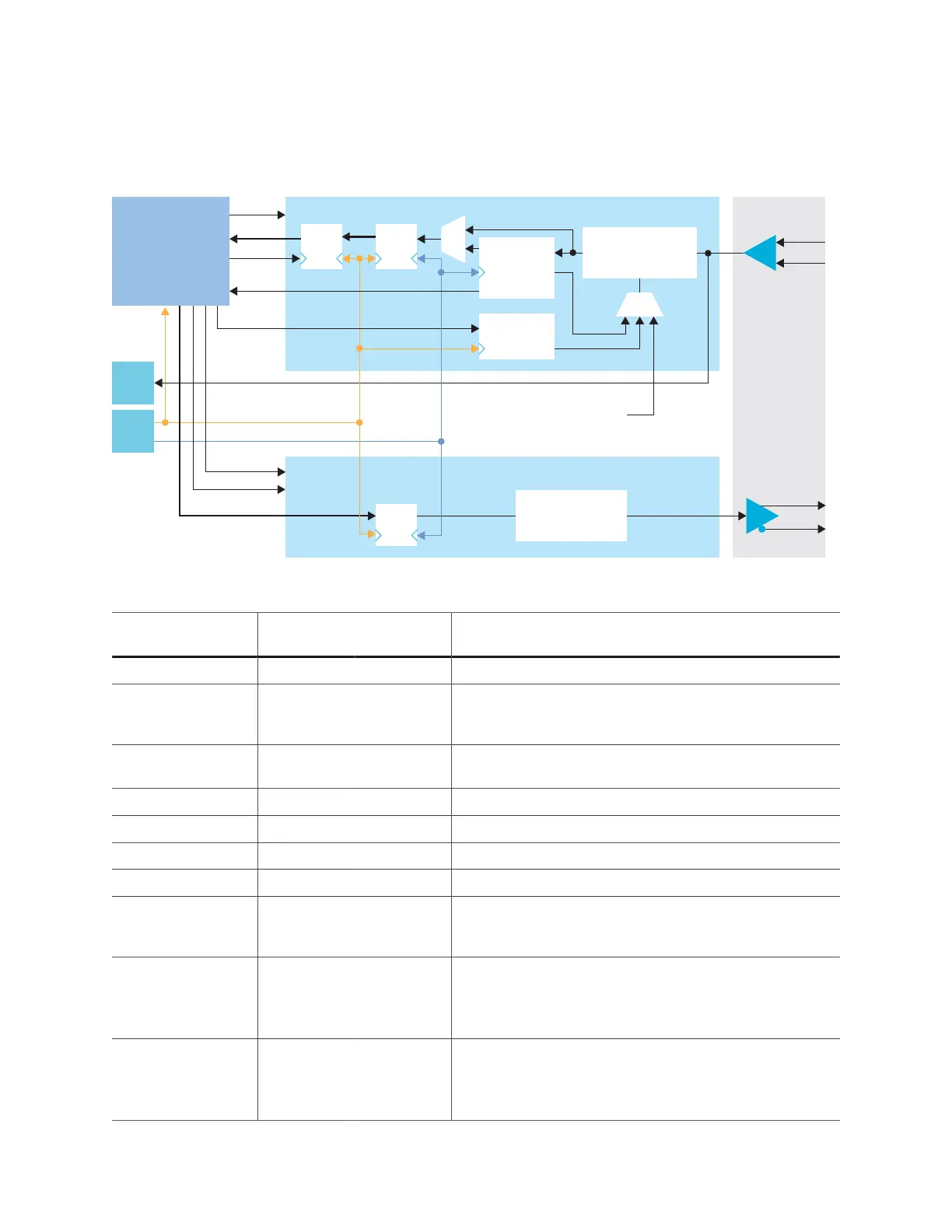
You can configure an HSIO block as one LVDS bidirectional signal. You must use the same
serialization for the RX and TX.
Figure 26: LVDS Bidirectional Interface Block Diagram
FIFO
Configuration
Setting
Serializer
TXP
TXN
OE
RST
OUT[n:0]
LVDS TX
Programmable
Delay
Table 40: LVDS Bidirectional Signals (Interface to FPGA Fabric)
Signal Direction Clock
Domain
Description
IN[9:0] Output SLOWCLK Parallel input data to the core. The width is programmable.
LOCK Output – (Optional) When DPA is enabled, this signal indicates
that the DPA has achieved training lock and data can be
passed.
FIFO_EMPTY Output FIFOCLK (Optional) When the FIFO is enabled, this signal indicates
that the FIFO is empty.
INSLOWCLK Input – Parallel (slow) clock for RX.
INFASTCLK Input – Serial (fast) clock for RX.
FIFOCLK Input – (Optional) Core clock to read from the FIFO.
FIFO_RD Input FIFOCLK (Optional) Enables FIFO to read.
INRST Input FIFOCLK
SLOWCLK
(Optional) Asynchronous. Resets the FIFO and RX serializer.
If the FIFO is enabled, it is relative to FIFOCLK; otherwise it
is relative to SLOWCLK.
ENA Input – Dynamically enable or disable the LVDS input buffer. Can
save power when disabled.
1: Enabled
0: Disabled
TERM Input – Enables or disables termination in dynamic termination
mode.
1: Enabled
0: Disabled
www.efinixinc.com 71