EasyManua.ls Logo

IMO HD2-3.7A-43 - Page 265

IMO HD2-3.7A-43
408 pages
Print Icon
To Next Page IconTo Next Page
To Previous Page IconTo Previous Page
Loading...
HD2 Series Inverter Function Parameter List
-256-
Function
code
Name
Description
Default
value
Modify
delay
P25.16
S7 terminal
switch-on delay
0.000s
P25.17
S7 switch-off
delay
0.000s
P25.18
S8 terminal
switch-on delay
0.000s
P25.19
S8 switch-off
delay
0.000s
P25.20
S9 terminal
switch-on delay
0.000s
P25.21
S9 switch-off
delay
0.000s
P25.22
S10 terminal
switch-on delay
0.000s
P25.23
S10 switch-off
delay
0.000s
P25.24
Lower limit value
of AI3
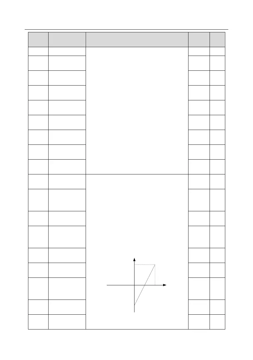
These function codes define the relation between
analog input voltage and corresponding set value
of analog input. When the analog input voltage
exceeds the range of max./min. input, the max.
input or min. input will be adopted during
calculation.
When analog input is current input, 0–20mA
current corresponds to 0–10V voltage.
In different application cases, 100% of the analog
setting corresponds to different nominal values.
The figure below illustrates several settings.
-100%
100%
Corresponding
setting
AI
10V
20mA
0
AI3/AI4
Input filter time: Adjust the sensitivity of analog
input, increase this value properly can enhance
0.00V
P25.25
Corresponding
setting of lower
limit of AI3
0.0%
P25.26
Upper limit value
of AI3
10.00V
P25.27
Corresponding
setting of upper
limit of AI3
100.0%
P25.28
Input filter time of
AI3
0.030s
P25.29
Lower limit value
of AI4
0.00V
P25.30
Corresponding
setting of lower
limit of AI4
0.0%
P25.31
Upper limit value
of AI4
10.00V
P25.32
Corresponding
setting of upper
100.0%

Table of Contents

Related product manuals