2-3
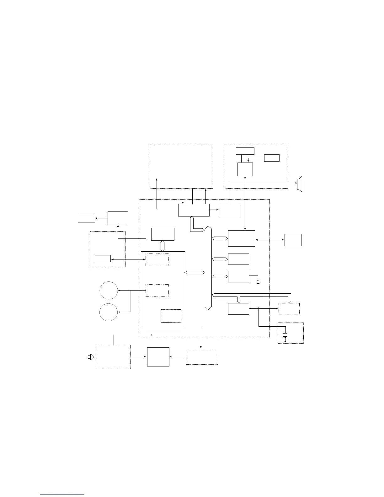
2.2 Main Control PCB
The main control PCB controls the operations of all machine functions.
Jumper JP1 on the main control PCB is used for battery back up of the SRAM. All user programmed
data and internal memory switch settings are held in SRAM. Removing JP1 will initialize the SRAM.
NOTE: JP1 should remain in the "ON" position at all times.
Memory (FLASH MEMORY, SRAM, SDRAM)
FLASH MEMORY --- T h e F L A S H M E M O R Y c o n t a i n s a l l p r o g r a m i n s t r u c t i o n s f o r u n i t operation.
SRAM --- T h e S R A M , w h i c h i s b a c k e d - u p b y a l i t h i u m b a t t e r y i s u s e d t o s t o r e u s e r p r o g r a m m e d
information.
SDRAM --- T h e S D R A M i s u s e d f o r b u f f e r , w h i c h i s b a c k e d - u p b y a b a t t e r y i s u s e d t o s t o r e
memorized documents.
NOTE: Turning parameters for Color(R,G,B) and Gray mode are stored in the EEPROM(IC42). When
the PCB MAIN is replaced, the EEPROM on malfunction PCB should be replaced to the new
PCB.
FBS
MOTOR
ADF
MOTOR
NCU PCB
TONE RXA TXA
DISPLAY
KEY
PANEL
G/A
PNAEL PCB
MODEM
MONITOR
CONTROL
CPU
USB
SRAM
SDRAM SDRAM
Ni-MH
H.V.POWER
SUPPLY UNIT
AC
PRINTER
CONTROL
MOTOR
CONTROL
IMAGE
PROCESS
CCD
SDRAM
INVERTERCCFL
CCD PCB
+24V,
+24V,
+5V,+3.3V
MAIN CONTROL PCB
CENECTOR-B PCB
Extention Memory
Lithium
+24V
+24V,+12V,AREF
FLASH
MEMORY
POWER SUPPLY
UNIT
PRINTER
UNIT
MFP
ENGINE
Main control PCB block diagram

 Loading...