Display
NVIDIA Jetson Nano DG-09502-001_v2.1 | 40
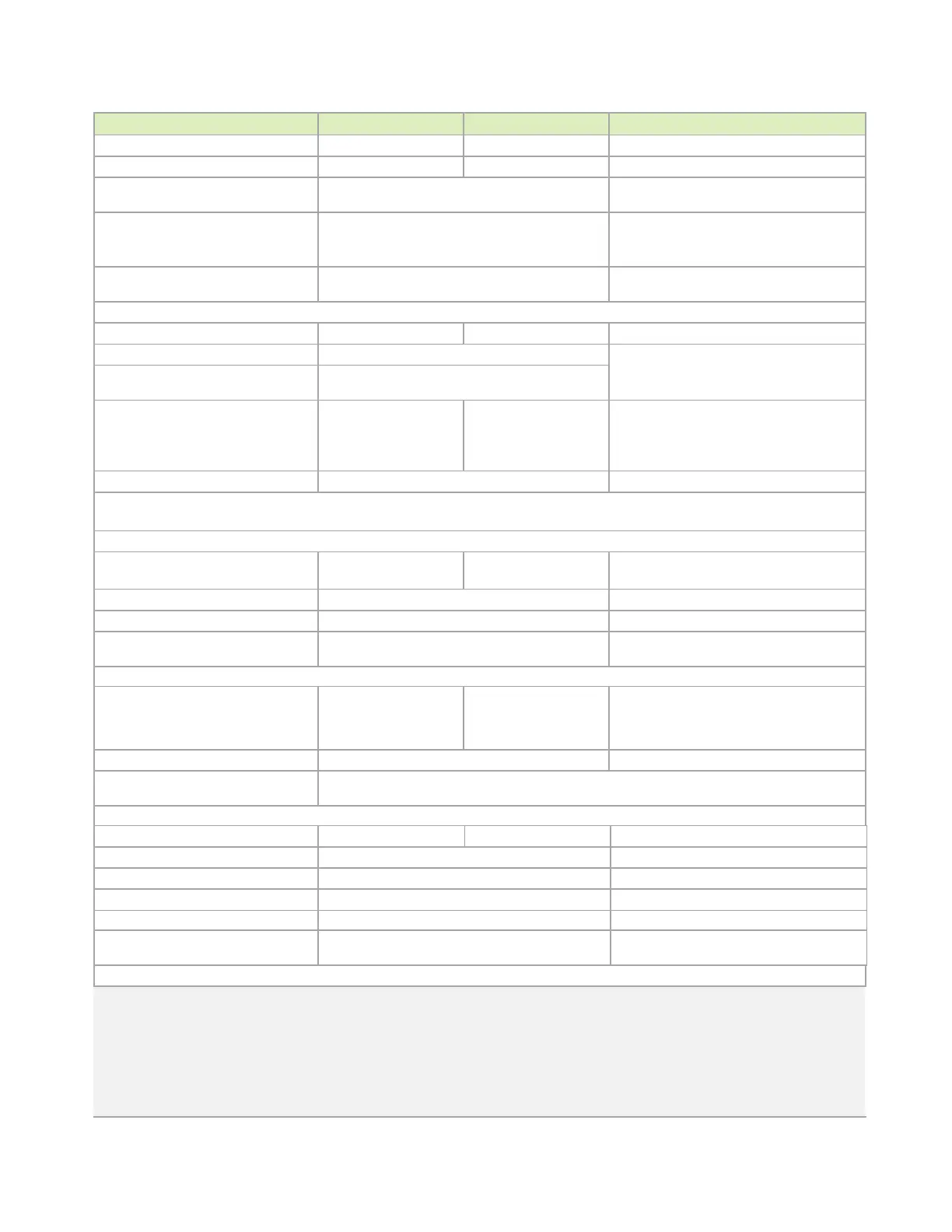
Parameter Requirement Units Notes
Value 0.1 uF
Max via distance from BGA 7.62 (52.5) mm (ps)
Location must be placed before pull-down resistor
The distance between the AC cap and the HDMI
connector is not restricted.
Placement PTH design
Micro-via design
Place cap on bottom layer if main-route above co re
Place cap on top l ayer if main-route bel ow core
Not Restricted
Void
GND (or PWR) void under/above the cap is needed. Void
size = SMT area + 1x dielectric height keepout distance
See Figure 7-14
Pull-down Resistor (RPD), choke/FET
Value 500 Ω
Location. Must be placed after AC cap Placement: See Figure 7-15
Layer of placement Same layer as AC cap. The FET and choke can be placed
on the opposite layer thru a PTH via
Choke between RPD and FET choke
Max trace Rdc
Max trace length
600 or
1
≤20
4
Ω @ 100 MHz
uH@DC-100 MHz
mΩ
mm
Can be choke or Trace. Recommended option for
HDMI2.0 HF1-9 improvement.
Void GND/PWR void under/above cap is preferred
Common-mode Choke (Not recommended – only used if absolutely required for EMI issues)
See Appendix A for details on CMC if implemented.
ESD (On-chip protection diode can withstand 2kV HMM. External ESD is optional. Designs should include ESD footprint as a stuffing option)
Max junction capacitance
(IO to GND)
0.35 pF e.g. Texas Instruments TPD4E02B04DQAR
Footprint Pad right on the net instead of trace stub See Figure 7-16
Location After pull-down resistor/CMC and before RS
Void GND/PWR void under/above the cap is needed. Void size =
1mm x 2mm for 1 pair
See Figure 7-17
Series Resistor (RS) – Series resistor on N/P path for HDMI 2.0 (mandatory)
Value ≤ 6 Ω ± 10%. 0ohm is acceptable if the design passes the
HDMI2.0 HF1-9 test. Otherwise, adjust the R
S va l ue
to ensure the HDMI2.0 tests pass: Eye diagram,
Vlow test and HF1-9 TDR test
Location After all components and before HDMI connector
Void GND/PWR void under/above the RS device is needed. Void size = SMT area + 1x dielectric height keepout
distance.
Trace at Component Region
Value 100 Ω ± 10%
Location At component region (Microstrip)
Trace entering the SMT pad One 45° See Figure 7-18
Trace between components Uncoupled structure See Figure 7-19
HDMI connector
Connector voiding Voiding the ground below the signal lanes 0.1448(5.7mil)
larger than the pin itself
See Figure 7-20
General: See C ha pte r 15 for guidelines related to Serpentine routing, routing over voids and noise coupling
Notes:
1. Longer trace lengths may be possible if the total trace loss is equal to or better than the target. If the loss is greater, the max trace lengths will need to be
reduced.
2. The average of the differential signals is used for length matching.
3. Do not perform length matching within breakout region. Recommend doing trace length matching to <1ps before vias or any discontinuity to minimize
common mode conversion
4. If routing includes a flex or 2nd PCB, the max trace delay and skew calculations must include all the PCBs/flex routing. Solut io ns wit h f l e x/2 nd P C B ma y
not achieve maximum frequency operation.

 Loading...


