114 www.xilinx.com Virtex-4 FPGA Configuration User Guide
UG071 (v1.12) June 2, 2017
Chapter 8: Readback and Configuration Verification
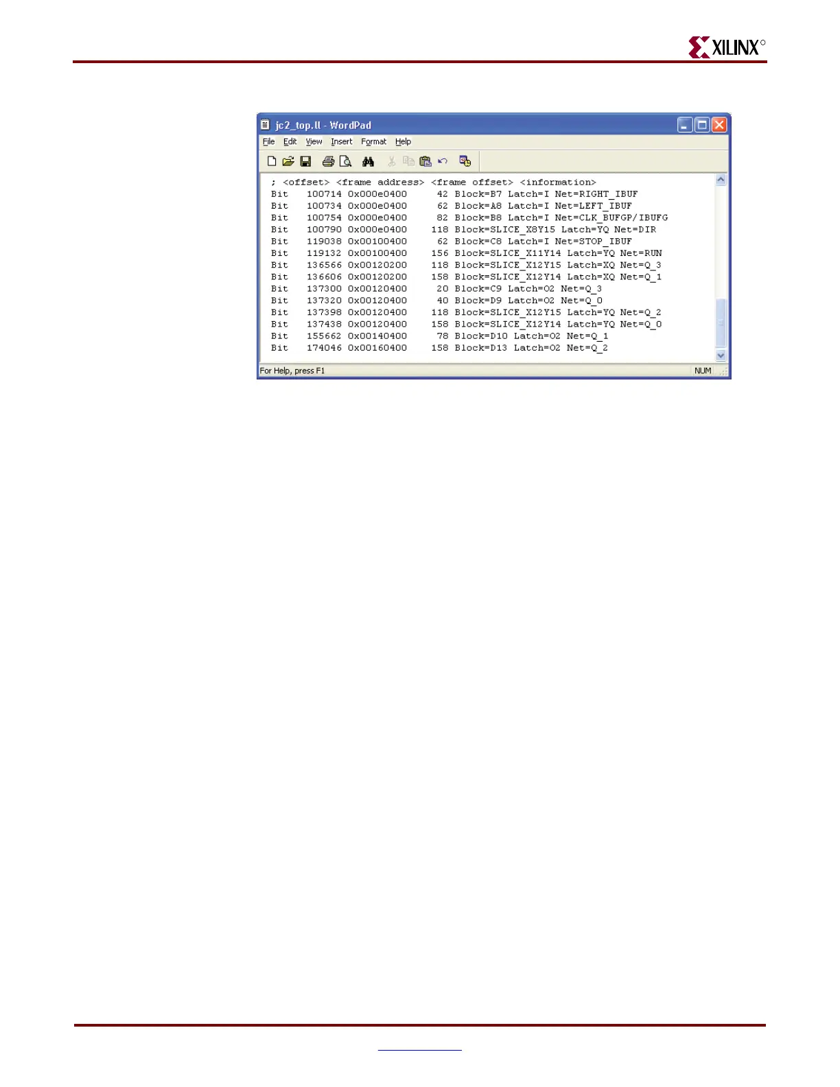
Figure 8-8 shows a snippet from a logic allocation file for the ISE jc2_top example design.
The line from the header comments explaining the line format has been moved to the start
of the bit offset data for clarity. The <offset> field gives the absolute bit offset from the
beginning of the readback frame data. The <frame address> field gives the frame address
that the capture bit is located in, and the <frame offset> field gives the bit offset from the
start of the frame. The <information> field gives the mapping between the bit and the user
design—for example, the DIR register (Figure 8-8) that is located in Slice X8Y15 is located
at bit offset 100790.
Note that captured DFF values, along with LUTRAM and SRL16 values, are stored in their
inverted sense.
Figure 8-8: Logic Allocation File Format

 Loading...


