UG-1828 Preliminary Technical Data
Rev. PrC | Page 288 of 338
VDIG_1P0 (L7,L8)
VDIGIO_1P8 (M7)
VDIG_0P9 (M8)
VCONV_1P8 (G7)
VAGPIO_1P8 (G8)
VANA1_1P8 (H13) +
External Tx1 pull-ups
VANA2_1P8 (H2) +
External Tx2 pull-ups
VRFSYN1_1P3 (E11)
VRFSYN2_1P3 (E4)
VAUXSYN_1P3 (E10)
VCLKSYN_1P3 (E5)
VRFVC01_1P3 (A10)
VRFVC02_1P3 (A5)
VCLKVCO_1P3 (G5)
VAUXVCO_1P3 (G10)
VANA1_1P3 (C8)
VANA2_1P3 (C7)
VRFVCO1_1P0 (B9)
VRFLO1_1P0 (A9)
VRFVCO2_1P0 (B6)
VRFLO2_1P0 (A6)
VCONV_1P3 (H8)
VRX1LO_1P3 (E13)
VRX2LO_1P3 (E2)
VTX1LO_1P3 (G12)
VTX2LO_1P3 (G3)
VCLKVCO_1P0 (H5)
VAUXVCO_1P0 (H10)
VCONV_1P0 (H7)
VRX1LO_1P0 (E14)
VRX2LO_1P0 (E1)
VTX1LO_1P0 (H12)
VTX2LO_1P0 (H3)
VANA2_1P0 (C6)
VANA1_1P0 (C9)
4.7µF
Not connected
4.7µF
Not connected
Standard operating
Configuration 0
All internal LDOs used
Internal LO generation used.
VDDA_1P3
2.5% tol.
VDDA_1P0
2.5% tol.
Internal PLLs not used for LOs.
LO GEN supply disconnected
and powered down internally.
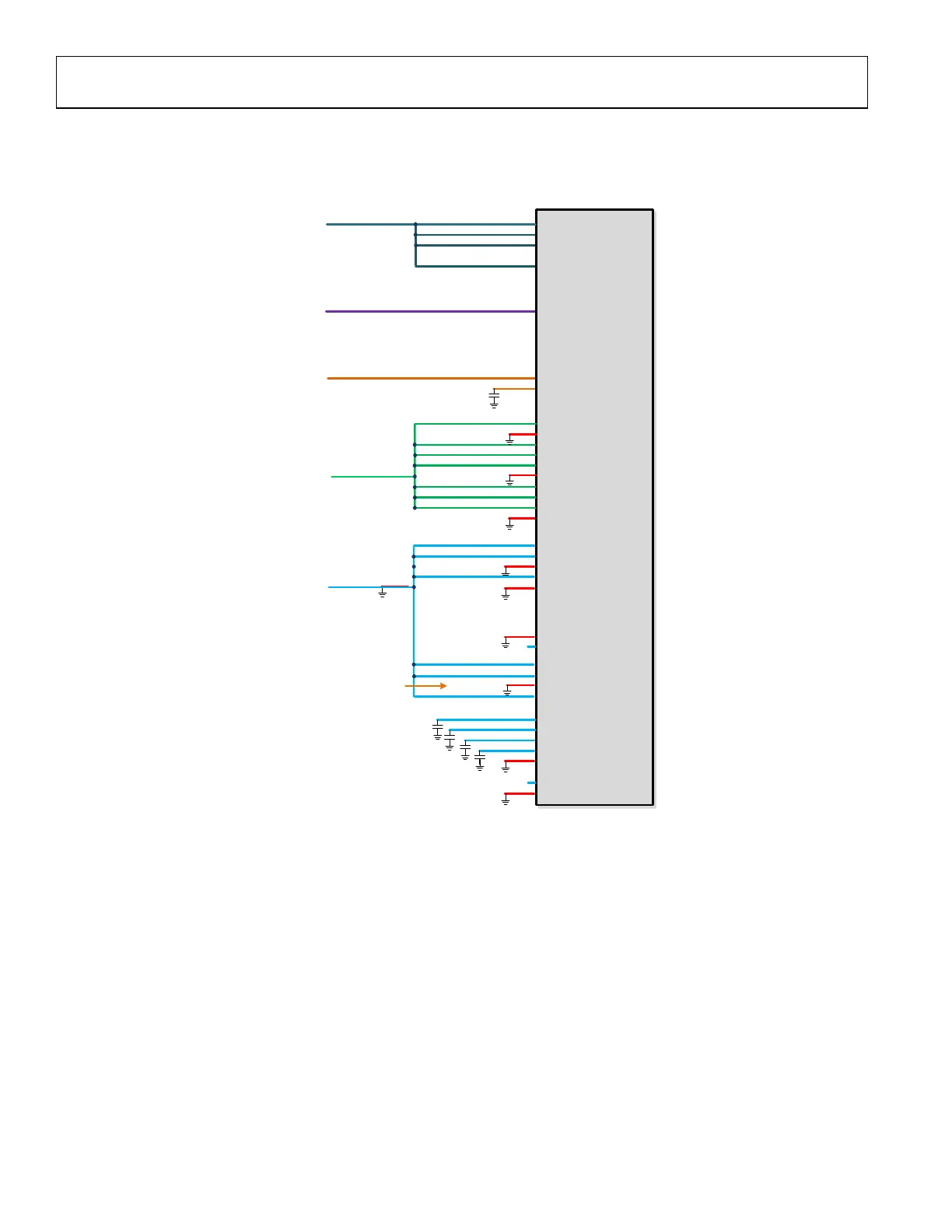
Figure 268. Tx1/Rx1 External LO Power Solution
Now that the hardware configuration is known the LDO configuration can be determined and the LDOs each set to the correct mode. In
this case the following table outlines the mode needed for each of the LDOs to prevent overvoltage failures or other unwanted errors.
Table 113. Example LDO Modes and Pin Mapping
LDO
Bypassed due to external 1.0v
Bypassed due to external 1.0v
Bypassed due to external 1.0v
Powered off, ch2 not required
Powered off, ch2 not required
 Loading...