UG-1828 Preliminary Technical Data
Rev. PrB | Page 78 of 277
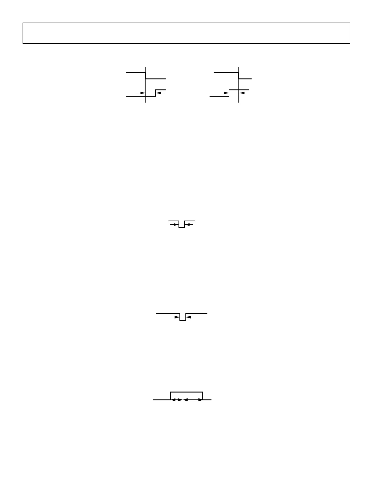
SETUP HOLD
24159-572
MCS
REF_CLK
SAMPLED
MCS
MCS SAMPLING USING POSITIVE EDGE OF REF_CLK
Figure 72 Sample MCS signal at rising edge of DEV_CLK
An external clock module is required to synchronize multiple ADRV9002 devices. Each ADRV9002 will receive a DEV_CLK and an
MCS signal. The MCS signals should arrive at all ADRV9002 devices within one DEV_CLK cycle, for the reason that it needs to be
sampled by the DEV_CLK mentioned above. For this reason, we recommend the layout to have equal-length traces between the external
clock module and each of the ADRV9002 devices. User will need to carefully tune the external clock module so that the pulses will arrive
at all ADRV9002 devices within one clock cycle time.
Setup time means the MCS positive edge has to arrive at least 5ns before DEV_CLK positive edge.
Hold time means the MCS negative edge has to arrive at least 5ns after DEV_CLK positive edge.
Setup/hold time are still being characterized and this is a preliminary result.
MCS pulses
The Figure 73 shows the MCS signal required to be received by ADRV9002. There are a total of 6 pulses. First 4 pulses are for the analog
clock divider synchronization, and the last 2 are for the digital clock divider synchronization. Together they will synchronize all internal
components of ADRV9002.
FIRST MCS
ANALOG
MCS
MCS
DEVICE CLOCK
DIVIDER
SYNCHRONIZATION
SECOND MCS
ANALOG
PLL REFERENCE
CLOCK DIVIDER
SYNCHRONIZATION
THIRD MCS
ANALOG
PLL STATE
MACHINE
SYNCHRONIZATION
FOURTH MCS
ANALOG
CLKGEN DIVIDER
SYNCHRONIZATION
FIRST MCS
DIGITAL
DIGITAL CLOCK
DIVIDER
SYNCHRONIZATION
SECOND MCS
DIGITAL
RX DATA
INTERFACE
SYNCHRONIZATION
24159-073
Figure 73 MCS pulses for analog and digital synchronization
Pulse width and delay
Table 31 shows the minimum pulse width of each MCS pulse, as well as the wait time required after each pulse. The user should use this
reference to design MCS pulse generation.
Table 31. Minimum Time Requirement for MCS Pulse Width and Wait Time
Pulse No. Pulse Width (No. of Reference Clock Cycles) Wait Time After the Pulse Tn (µs)
1 ≥2 >1
2 ≥2 >1
3 ≥2 >1
4 ≥2 >100
5 ≥2 >100
6 ≥2 >1
 Loading...