Model 3580A
GENERAL
OPERATING
INFORMATION
Section III
3-37.
Overload
Indicator.
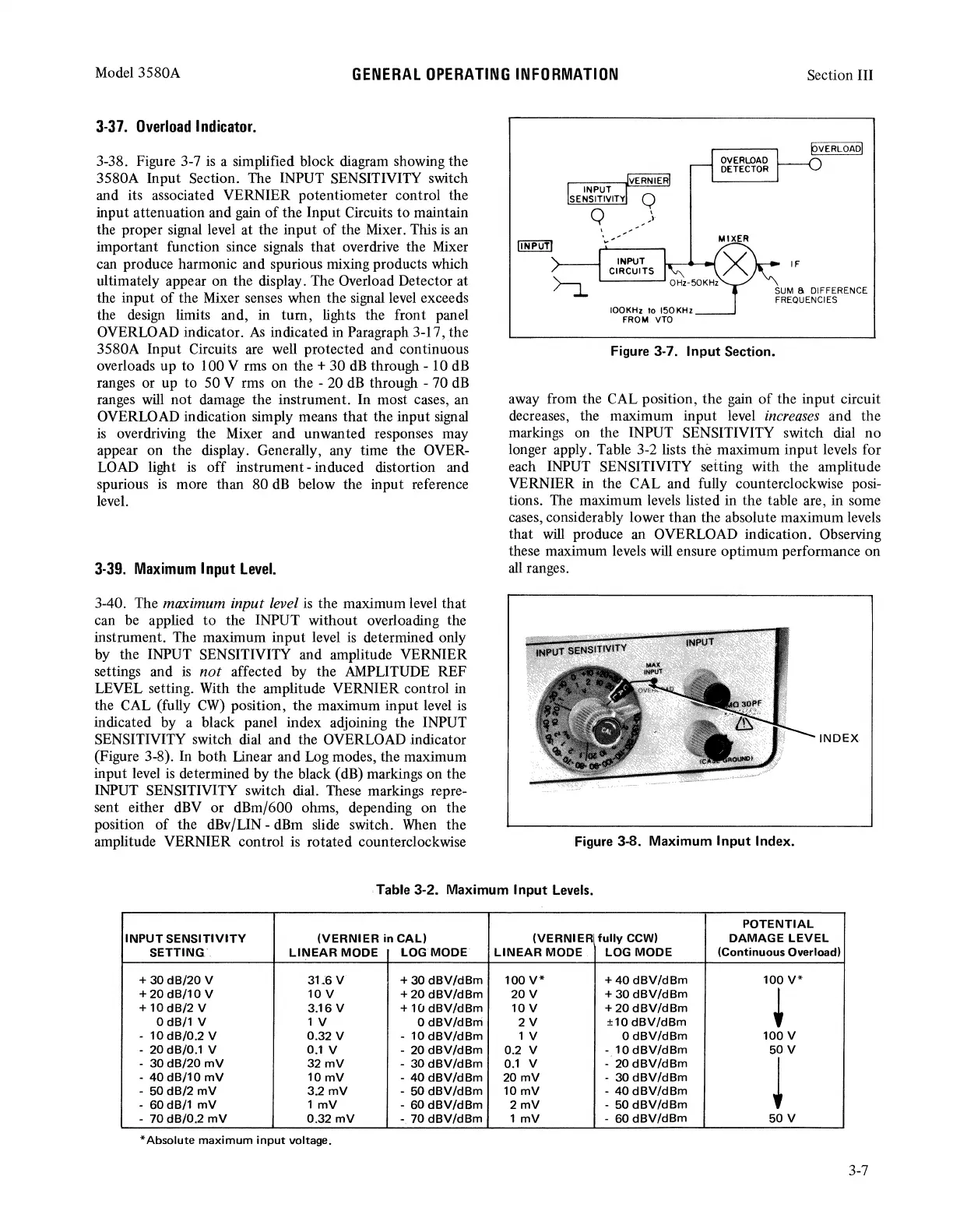
3-38. Figure 3-7
is
a simplified block diagram showing the
3580A Input Section. The INPUT SENSITIVITY switch
and its associated VERNIER potentiometer control the
input attenuation and gain
of
the Input Circuits to maintain
the proper signal level at the input
of
the Mixer. This
is
an
important function since signals that overdrive the Mixer
can produce harmonic and spurious mixing products which
ultimately appear on the display. The Overload Detector at
the input
of
the Mixer senses when the signal level exceeds
the design limits and, in turn, lights the front panel
OVERLOAD indicator.
As
indicated in Paragraph 3-17, the
3580A Input Circuits are well protected and continuous
overloads up to 100 V rms on the + 30
dB
through - 10
dB
ranges or up
to
50 V rms on the - 20
dB
through - 70
dB
ranges will
not
damage the instrument. In most cases, an
OVERLOAD indication simply means that the input signal
is
overdriving the Mixer
and
unwanted responses may
appear on the display. Generally, any time the OVER-
LOAD light
is
off
instrument -induced distortion and
spurious
is
more than 80
dB
below the input reference
level.
3-39.
Maximum
Input
Level.
3-40. The maximum input level
is
the maximum level that
can be applied
to
the INPUT without overloading the
instrument. The maximum input level
is
determined only
by the INPUT SENSITIVITY and amplitude VERNIER
settings and
is
not
affected by the AMPLITUDE REF
LEVEL setting. With the amplitude VERNIER control in
the CAL (fully
CW)
position, the maximum input level
is
indicated by a black panel index adjoining the INPUT
SENSITIVITY switch dial and the OVERLOAD indicator
(Figure 3-8). In
both
Linear and Log modes, the maximum
input level
is
determined by the black (dB) markings on the
INPUT SENSITIVITY switch dial. These markings repre-
sent either dBV or dBm/600 ohms, depending on the
position
of
the dBv/LIN - dBm slide switch.
When
the
amplitude VERNIER control
is
rotated counterclockwise
\
..........
...
INPUT
CIRCUITS
IOOKHz to 150 KHz
FROM
VTO
OVERLOAD
DETECTOR
MIXER
IF
SUM
8 DIFFERENCE
FREQUENCIES
Figure 3-7. Input Section.
away from the CAL position, the gain
of
the input circuit
decreases, the maximum input level increases and the
markings on the INPUT SENSITIVITY switch dial no
longer apply. Table 3-2 lists
the
maximum input levels for
each INPUT SENSITIVITY setting with the amplitude
VERNIER in the CAL and fully counterclockwise posi-
tions. The maximum levels listed in the table are, in some
cases, considerably lower than the absolute maximum levels
that will produce an OVERLOAD indication. Observing
these maximum levels will ensure optimum performance on
all
ranges.
INDEX
Figure 3-8. Maximum Input Index.
Table 3-2. Maximum Input Levels.
POTENTIAL
INPUT
SENSITIVITY
(VERNIER
in
CALI
(VERNIER
fully CCWI
DAMAGE
LEVEL
SETTIN.G.
LINEAR
MODE
LOG MODE
LINEAR
MODE
LOG
MODE
(Continuous Overload)
+
30d8/20
v
3L6V
+
30dBV/dBm
100
V*
+
40
dBV/dBm
100
V*
+
20
dB/10
V
10
v
+20
dBV/dBm
20V
+30dBV/dBm
~
+
10
dB/2
V 3.16 v +
1CJ
dBV/dBm
10
v
+20dBV/dBm
0 dB/1 V 1 v
0 dBV/dBrri
2V
±10dBV/dBm
-
10
dB/0.2
V
0.32 v
- 10
dBV/dBm
1 v
OdBV/dBm
100 v
- 20 dB/0.1 V
0.1
v -
20dBV/dBm
0.2 v -
10
dBV/dBm
50V
-
30dB/20
mV
32mV
- 30
dBV/dBm
0.1
v -
20dBV/dBm
!
-
40
dB/10
mV
10
mV
-
40
dBV/dBm
20
mV
-
30dBV/dBm
-
50dB/2
mV
3.2mV
-
50dBV/dBm
10
mV
-
40dBV/dBm
-
60dB/1
mV
1
mV
- 60
dBV/dBm
2mV
- 50
dBV/dBm
- 70
dB/0.2
mV
0.32 rnV - 70
dBV/dBm
1
mV
- 60
dBV/dBm
50 v
*Absolute
maximum
input
voltage.
3-7