Section IV
START
TRA
M•OA-1-1572
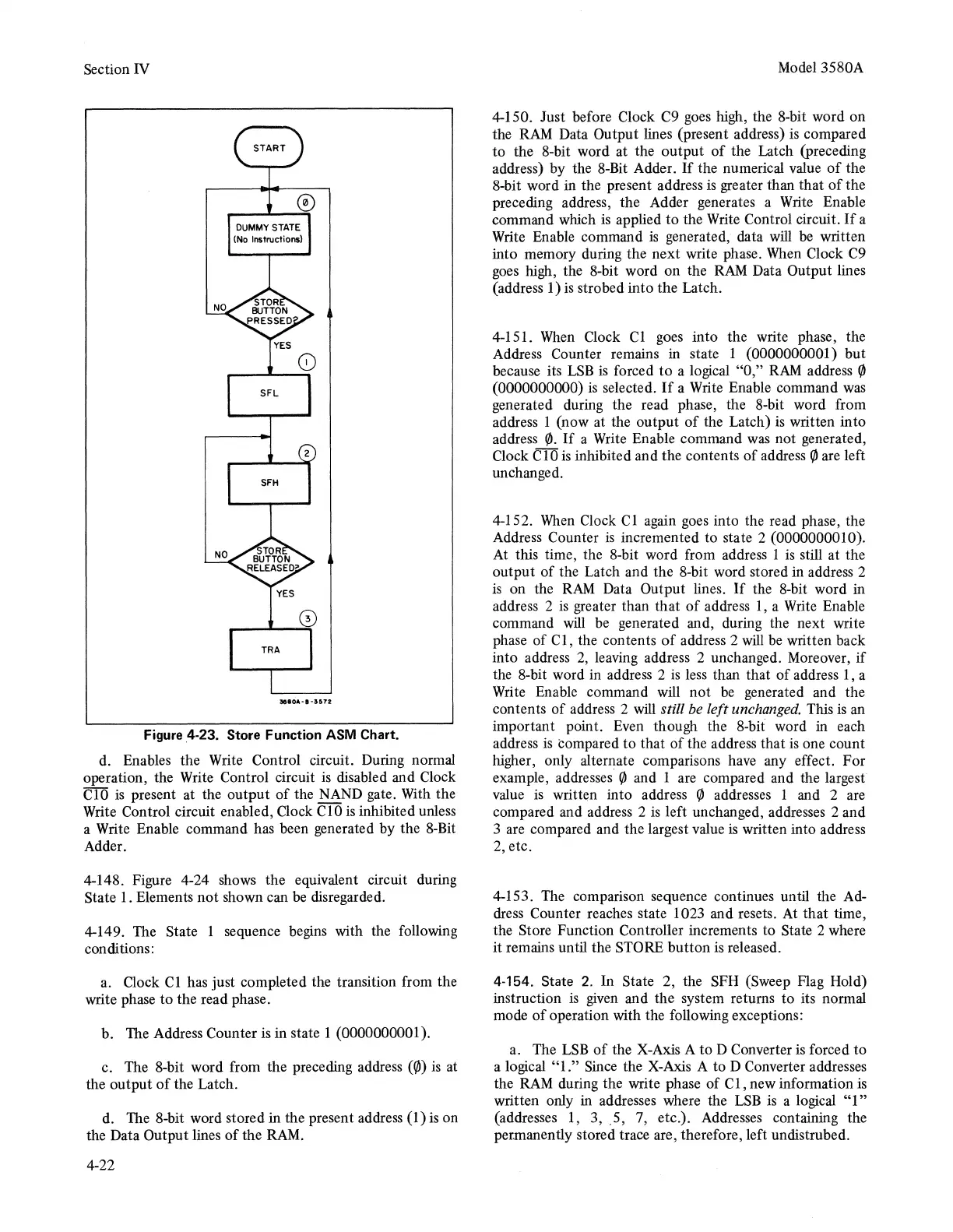
Figure
.4-23.
Store Function ASM Chart.
d. Enables the Write Control circuit. During normal
operation, the Write Control circuit is disabled and Clock
ClO
is
present at the output
of
the NAND gate. With the
Write Control circuit enabled, Clock ClO
is
inhibited unless
a Write Enable command has been generated by the 8-Bit
Adder.
4-148. Figure 4-24 shows the equivalent circuit during
State 1. Elements
not
shown can be disregarded.
4-149. The State 1 sequence begins with the following
conditions:
a. Clock
Cl
has just completed the transition from the
write phase
to
the read phase.
b. The Address Counter is in state 1 (0000000001).
c. The 8-bit word from the preceding address (0)
is
at
the output
of
the Latch.
d. The 8-bit word stored in the present address (1)
is
on
the Data Output lines
of
the
RAM.
4-22
Model 3580A
4-150. Just before Clock C9 goes high, the 8-bit word on
the
RAM
Data Output lines (present address) is compared
to the 8-bit word at the
output
of
the Latch (preceding
address) by the 8-Bit Adder.
If
the numerical value
of
the
8-bit word in the present address
is
greater than
that
of
the
preceding address, the Adder generates a Write Enable
command which
is
applied
to
the Write Control circuit.
If
a
Write Enable command
is
generated, data will
be
written
into memory during the next write phase. When Clock
C9
goes high, the 8-bit word on the
RAM
Data Output lines
(address 1)
is
strobed into the Latch.
4-151.
When
Clock Cl goes into the write phase, the
Address Counter remains in state 1 (0000000001)
but
because its
LSB
is
forced
to
a logical "O,"
RAM
address 0
(0000000000)
is
selected.
If
a Write Enable command
was
generated during the read phase, the 8-bit word from
address 1 (now at the output
of
the Latch)
is
written into
address
0.
If
a Write Enable command
was
not generated,
Clock C 10
is
inhibited and the contents
of
address 0 are left
unchanged.
4-152.
When
Clock C 1 again goes into the read phase, the
Address Counter
is
incremented to state 2 (0000000010).
At this time, the 8-bit word from address 1
is
still at the
output
of
the Latch and the 8-bit word stored in address 2
is
on the
RAM
Data Output lines.
If
the 8-bit word in
address 2
is
greater than that
of
address
1,
a
Write
Enable
command
will
be
generated and, during the next write
phase
of
Cl,
the contents
of
address 2
will
be
written back
into address
2,
leaving address 2 unchanged. Moreover,
if
the 8-bit word in address 2
is
less than that
of
address 1, a
Write Enable command will not
be
generated and the
contents
of
address 2 will still be
left
unchanged. This
is
an
important point. Even though the 8-bit word in each
address
is
compared
to
that
of
the address that
is
one count
higher, only alternate comparisons have any effect.
For
example, addresses 0 and 1 are compared and the largest
value is written into address 0 addresses 1 and 2 are
compared and address 2
is
left unchanged, addresses 2 and
3 are compared and the largest value
is
written into address
2, etc.
4-153. The comparison sequence continues until the Ad-
dress Counter reaches state 1023 and resets. At
that
time,
the Store Function Controller increments to State 2 where
it
remains until the STORE
button
is released.
4-154. State
2.
In State 2, the SFH (Sweep Flag Hold)
instruction
is
given
and the system returns to its normal
mode
of
operation with the following exceptions:
a. The
LSB
of
the X-Axis A
to
D Converter is forced to
a logical
"l
."
Since the X-Axis A to D Converter addresses
the
RAM
during the write phase
of
Cl,
new information
is
written only in addresses where the
LSB
is a logical
"l"
(addresses 1, 3, .5, 7, etc.). Addresses containing the
permanently stored trace are, therefore, left undistrubed.