Model 3580A Section VII
SECTION
VII
TROUBLESHOOTING
AND
CIRCUIT
7-1.
INTRODUCTION.
7-2. This section
of
the manual contains troubleshooting
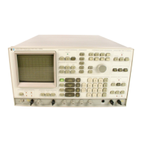
information and circuit diagrams for the Model 3580A
Spectrum Analyzer. Included are troubleshooting informa-
tion, information on factory selected components, func-
tional block diagrams, schematic diagrams and component
location diagrams.
7-3.
TROUBLESHOOTING
AND
PREVENTIVE
MAIN-
TENANCE.
7-4.
General
Troubleshooting
Procedures.
7-5. Troubleshooting information for the 3580A can be
found
in
the functional block diagrams and circuit diagrams
at the end
of
Section VII.
An
extensive set
of
notes,
waveforms, and tables has been provided to help narrow the
problems down from the functional block, to a board, and
finally to a component.
7-6.
Use
the Overall Functional Block Diagram (Figure 7-1)
to narrow the 3580A problem down into one
of
the four
major functional blocks:
1) Input Section
2) Frequency and Sweep Section
3)
IF Section
4) Display Section.
lhis
diagram
gives
a good overall look at the 3580A
operation. Once the diagram
is
understood, the failure
symptoms alone may
be
adequate to lead you to the proper
block. Other times, the output signals from the 3580A will
suffice. For instance, the RECORDER X-AXIS and Y-AXIS
outputs
give
an indication
of
proper instrument operation
up to, but
not
including, the
A7
Logic
Board. The
TRACKING
OSC
OUTPUT indicates
if
the Frequency and
Sweep Section
is
working properly.
7-7.
If
the external control signals and front panel failure
symptoms are
not
adequate
to
localize a problem to a
particular block, remove the 3580A outer covers and check
the appropriate input and output lines
of
each block. This
will
localize the problem
to
a block. The Analog Block
Diagram (Figure 7-2), circuit schematics and associated
notes can then be used
to
isolate the problem
to
the
component.
DIAGRAMS
7-8.
A2
Board
VTO
Troubleshooting.
7-9. The
A2
VTO
is
part of a complex feedback loop.
If
the VTO circuitry
is
not working properly, the feedback
loop can
be
broken
by
applying approximately - 1.6 V
de
to A2TP4. A 0
to
+ 9 V
de
signal supplied to the VTO
ERROR
AMP
on the RED jumper lead
to
the
A2
board
should then cause the oscillator frequency
to
vary from 1.0
to 1.5
MHz
(Oto
50 kHz Input Frequency). This signal can
then
be
followed around the feedback loop
to
find the
faulty components.
Use
the waveforms supplied with the
A2
board to aid in this process.
7-1
0.
AJ
Board
T
rou
blesho
oti
ng.
7-11.
This
part
of
Section VII contains test procedures for
the digital control circuitry
of
the
A3
Sweep Board
(Schematic 4).
If
the previous troubleshooting procedures
indicate problems with the normal or adaptive sweep
circuitry, perform these test procedures.
a.
Position the 3580A front panel controls to:
SWEEP
MODE
.....................
REP
Short
A3TP1
to the gray jumper wire connected near the
center
of
the
A3
board (Don't remove the gray jumper).
b. Adjust A3R54 (INTEGRATOR BALANCE) to verify
that the output
of
the Ramp Integrator (A3TP1) can
be
adjusted from a positive
to
negative
de
voltage. Readjust
A3R54 for 0.000 volts ± .001 volts.
c. Measure
Vsg
on the dual FET, A3QI. Both FET's
should
have
Vsg
..;;;
3 V
de.
d. Set switch SI
to
the test position (UP position).
Verify that CLOCK OUTPUT (A3U8 pin 11)
is
a TTL
HIGH(;;;. 2.0 V de). Return SI
to
the normal position.
e. Remove the clock test jumper between
Q18
and
SI.
Reposition:
SWEEP
MODE
...................
RESET
f. Connect a logic clip to A3U5. Turn the 3580A
POWER switch OFF then back to ON. The instrument
CBA
should come up
in
state 000 or 100, where the
C, B,
and A
state outputs are located on pins 13, 14 and 15 respectively
of
A3U5.
If
the instrument comes up in state 000, clock it
to state 100
by
momentarily switching A3Sl into, and then
out
of
the test position. (This process
will
be
called
"clocking
Sl"
from now on.)
7-1