Model
3580A
OV
TO
+4.75V
VIDEO
(FROM
VIDEO
OUTPUT
CIRCUITS)
ov
TO
+sv
RAMP
(FROM
LINEAR
SWEEP
GENERATOR)
CLK
CiQ
READ/WRITE
RAM
(1024X8)
ADDRESS
10
----1
B
,__
__
_
I
T
s
ADDRESS
MULTIPLEXER
READ
CLOCK
.....__1_0_0_1r_s
_
_,
~g~~~~~
CARRY
r===DISPLAY
SECTION====.
LINE
GENERATOR
SAMPLE
(CLK
C7)
PIO
AB
OV
TO
+4.75V
RESTORED
VIDEO
Section IV
CLK
Cl
'---H-0--"R~c:.:~~:;o~'---TA_L~
(
H)
o~s:MLPA
y
"'"'
""'""""
)l
"'
--i.15-!8
mHc....fl_
CLK I
CLK
2
CLK
3
CLK
5
CLK
6
CLK 7
CLK
9
CLK
10
CLK
11
i..-
15-10
i''"...i
CLK CI
___f;ffiE~
C LK
C9
_________fl__
CLK CID
____Il__
CLK
Cl I
____
IL
j.-15-IBmm
---j
OV
DISPLAY
RAMP
3580A-C-3569
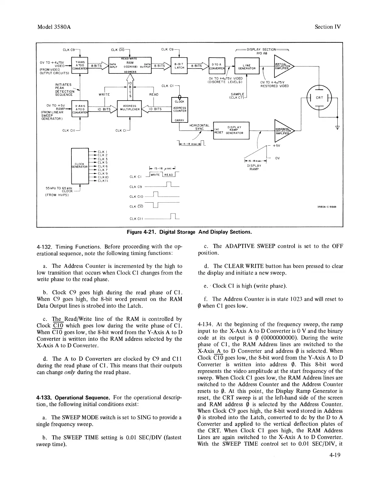
Figure 4-21. Digital Storage And Display Sections.
4-132. Timing Functions. Before proceeding with the op-
erational sequence, note the following timing functions:
a.
The Address Counter
is
incremented by the high to
low transition that occurs when Clock
Cl
changes from the
write phase to the read phase.
b. Clock
C9
goes high during the read phase
of
Cl.
When
C9
goes
high, the 8-bit word present on the
RAM
Data Output lines
is
strobed into the Latch.
c.
The Read/Write line
of
the
RAM
is
controlled by
Clock ClO which goes low during the write phase
of
Cl.
When
ClO goes low, the 8-bit word from the Y-Axis A to D
Converter
is
written into the
RAM
address selected by the
X-Axis
A to D Converter.
d.
The A to D Converters are clocked by
C9
and C
11
during the read phase
of
Cl.
This means that their outputs
can change only during the read phase.
4-133. Operational Sequence. For the operational descrip-
tion, the following initial conditions exist:
a.
The
SWEEP
MODE
switch
is
set to SING
to
provide a
single
frequency sweep.
b. The
SWEEP
TIME
setting
is
0.01 SEC/DIV (fastest
sweep time).
c.
The
ADAPTIVE
SWEEP
control
is
set to the OFF
position.
d.
The
CLEAR
WRITE
button has been pressed to clear
the display and initiate a new sweep.
e.
'Clock Cl
is
high (write phase).
f. The Address Counter
is
in state 1023 and will reset to
r/J
when C 1 goes low.
4-134.
At
the beginning
of
the frequency sweep, the ramp
input to the X-Axis A to D Converter
is
0 V and the binary
code at its output
is
r/J
(0000000000). During the write
phase
of
C 1, the
RAM
Address lines are switched to the
X-Axis
A
to
D Converter and address
r/J
is
selected.
When
Clock ClO
goes
low, the 8-bit word from the Y-Axis A to D
Converter
is
written into address
r/J.
This 8-bit word
represents the video amplitude at the start frequency
of
the
sweep.
When
Clock
Cl
goes
low, the
RAM
Address lines
are
switched to the Address Counter and the Address Counter
resets to
r/J.
At
this point, the Display Ramp Generator
is
reset, the CRT sweep
is
at the left-hand side
of
the screen
and
RAM
address
r/J
is
selected by the Address Counter.
When
Clock
C9
goes high, the 8-bit word stored in Address
r/J
is
strobed into the Latch, converted
to
de
by
0
the D
to
A
Converter and applied
to
the vertical deflection plates
of
the CRT.
When
Clock
Cl
goes
high, the
RAM
Address
Lines
are
again
switched to the
X-Axis
A
to
D Converter.
With
the
SWEEP
TIME control set
to
O.ol SEC/DIV, it
4-19