Section IV
Model
3580A
CLK
CIO
CLK
C9
READ/WRITE
Q
DATA
RAM
DATA
8 BITS
8-BIT
INPUT
(1024X8
OUTPUT
LATCH
14-11,us
--j
CLKCI~
CLKC9____fl__
CLKCIO__Jl__
CLKCiO--u---
3580A-B-357'4
ADDRESS
10
BITS
Q
m
8 BITS
DTOA
CONVERTER
CLK Cl
CLOCK
SFL+TRA
ADDRESS
SFH
COUNTER
BLANK
STORE
CARRY
CLEAR
HORIZONTAL
'--~~~~~~---SYNC
l--11.4m1
---IL
(TO
DISPLAY
RAMP
GENERATOR)
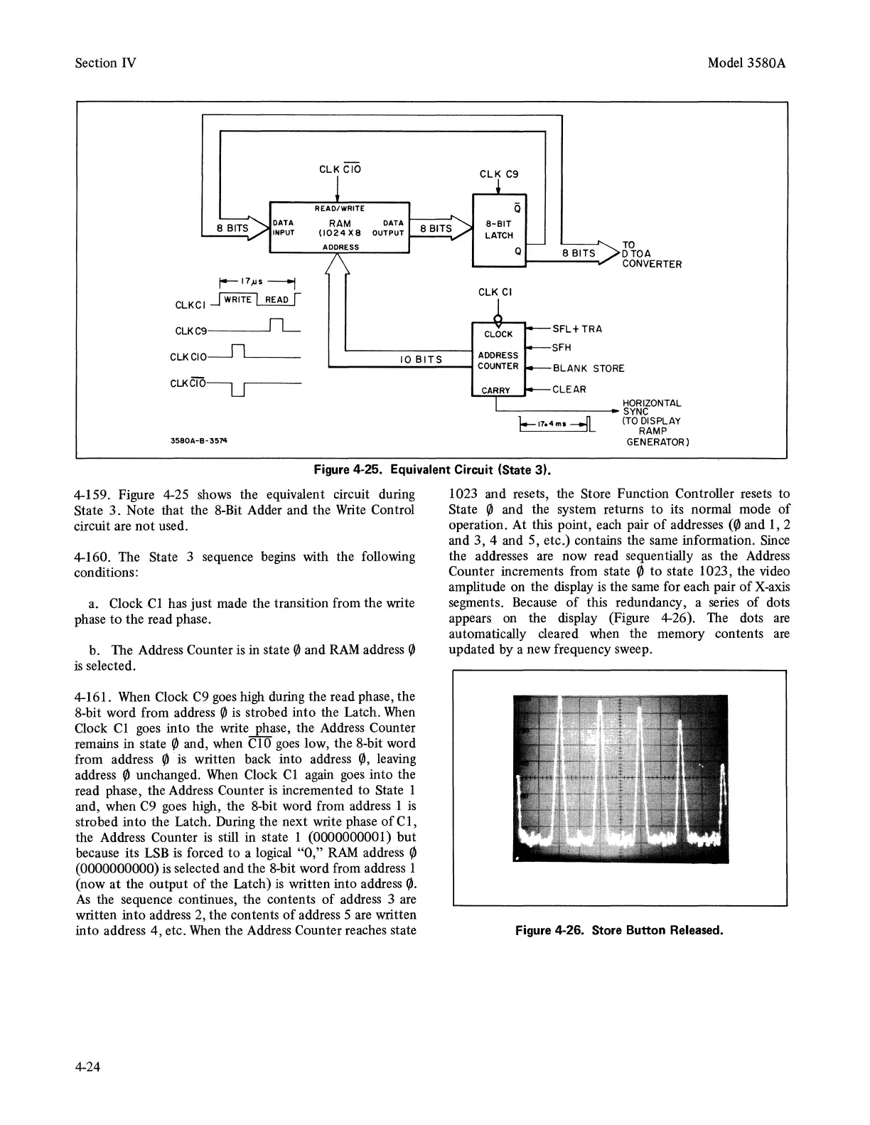
Figure 4-25. Equivalent Circuit (State 3).
4-159. Figure 4-25 shows the equivalent circuit during
State 3. Note that the
8-Bit
Adder and the
Write
Control
circuit are not used.
4-160. The State 3 sequence
begins
with the following
conditions:
a. Clock
Cl
has just made the transition from the write
phase
to
the read phase.
b. The Address Counter
is
in state
</J
and
RAM
address
'/J
is selected.
4-161.
When
Clock
C9
goes
high during the read phase, the
8-bit word from address
</J
is
strobed into the Latch.
When
Clock Cl
goes
into the write phase, the Address Counter
remains in state
</J
and, when ClO
goes
low, the 8-bit word
from address
</J
·is written back into address
'/J,
leaving
address
</J
unchanged.
When
Clock Cl
again
goes
into the
read phase, the Address Counter
is
incremented to State 1
and, when
C9
goes
high, the 8-bit word from address 1
is
strobed into the Latch. During the next write phase
of
Cl,
the Address Counter
is
still in state 1 (0000000001)
but
because its
LSB
is
forced to a logical "O,"
RAM
address
</J
(0000000000)
is
selected and the 8-bit word from address 1
(now
at
the output
of
the Latch)
is
written into address
(/J.
As
the sequence continues, the contents
of
address 3
are
written into address 2, the contents
of
address 5
are
written
into address 4, etc.
When
the Address Counter reaches state
4-24
1023 and resets, the Store Function Controller resets to
State
'/J
and the system returns
to
its normal mode
of
operation. At this point, each pair
of
addresses
(</J
and 1, 2
and 3, 4 and 5, etc.) contains the same information.
Since
the addresses
are
now read sequentially
as
the Address
Counter increments from state
</J
to state 1023, the video
amplitude on the display
is
the
same
for each pair
of
X-axis
segments. Because
of
this redundancy, a
series
of
dots
appears
on
the display (Figure 4-26).
The
dots
are
automatically cleared when the memory contents
are
updated by a new frequency sweep.
Figure 4-26. Store Button Released.