Model 3580A
sweep
is
made, the trace that
is
generated will continue to
be
displayed until it
is
cleared or updated by a new sweep.
c.
If
a trace
is
needed for future reference, it can
be
permanently stored in memory
by
pressing the STORE
button. The permanently stored trace and a current or
"refresh" trace can then
be
displayed simultaneously.
d.
Display adjustments are not required when the sweep
parameters
are
changed. The digitally stored trace
is
automatically cleared and updated at the correct rate. The
INTENSITY and FOCUS controls
have
the same effect
as
those of a regular oscilloscope. Once they
are
set, they
do
not need
to
be
readjusted.
e. Digital storage provides a bright, crisp flicker-free
presentation. There
is
no blooming or display ambiguity.
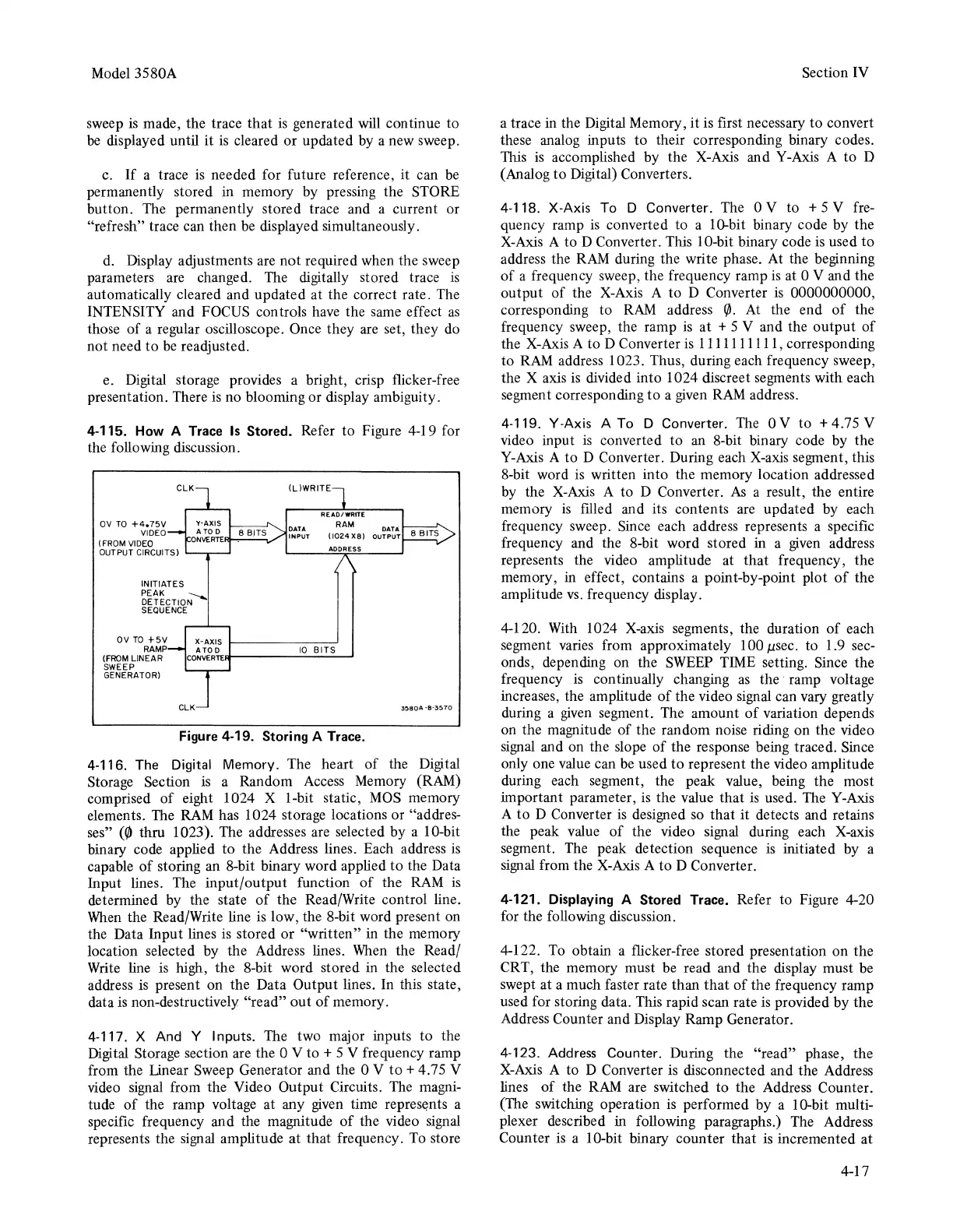
4-115. How A
Trace
Is
Stored. Refer to Figure 4-19 for
the following discussion.
CLK
OV
TO
+4o75V
VIDEO
(FROM
VIDEO
Y-AXIS~-•~
ATOD
ONVERTE......,.-~__,
OUTPUT CIRCUITS)
~...--~
INITIATES
:;g~cT10N-
SEQUENcE
OV
TO
+5V
RAMP
(FROM
LINEAR
SWEEP
GENERATOR)
(L)WRITE
READ/WRITE
RAM
DATA,__--.._
( 1024
XB)
OUTPUTr--8
B_IT....,s_,
ADDRESS
10
BITS
3~80A-B·3~70
Figure
4-19. Storing A Trace.
4-116. The Digital Memory. The heart
of
the Digital
Storage Section
is
a Random
Access
Memory (RAM)
comprised
of
eight 1024 X 1-bit static,
MOS
memory
elements. The
RAM
has 1024 storage locations or "addres-
ses"
(r/J
thru 1023). The addresses are selected by a 10-bit
binary code applied to the Address lines. Each address
is
capable
of
storing an 8-bit binary word applied
to
the Data
Input lines. The input/output function
of
the
RAM
is
determined by the state
of
the Read/Write control line.
When
the Read/Write line
is
low, the 8-bit word present on
the Data Input lines
is
stored or "written" in the memory
location selected by the Address lines.
When
the Read/
Write
line
is
high, the 8-bit word stored in the selected
address
is
present on the Data Output lines. In this state,
data
is
non-destructively "read"
out
of
memory.
4-117. X
And
Y Inputs. The two major inputs
to
the
Digital Storage section are the 0 V
to+
5 V frequency ramp
from the Linear Sweep Generator and the 0 V
to+
4.75 V
video signal from the Video Output Circuits. The magni-
tude
of
the ramp voltage at any
given
time repres(lnts a
specific frequency and the magnitude
of
the video signal
represents the signal amplitude at that frequency.
To
store
Section IV
a trace in the Digital Memory, it
is
first necessary
to
convert
these analog inputs to their corresponding binary codes.
This
is
accomplished by the X-Axis and
Y-Axis
A to D
(Analog
to
Digital) Converters.
4-118.
X-Axis
To
D Converter. The 0 V to + 5 V
fre-
quency ramp
is
converted to a 10-bit binary code by the
X-Axis
A to D Converter. This 10-bit binary code
is
used
to
address the
RAM
during the write phase. At the beginning
of
a frequency sweep, the frequency ramp
is
at 0 V and the
output
of
the
X-Axis
A
to
D Converter
is
0000000000,
corresponding to
RAM
address
f/J.
At
the end
of
the
frequency sweep, the ramp
is
at
+ 5 V and the output
of
the
X-Axis
A to D Converter
is
1111111111, corresponding
to RAM address 1023. Thus, during each frequency sweep,
the X axis
is
divided into 1024 discreet segments with each
segment corresponding
to
a
given
RAM
address.
4-119. Y
-Axis
A To D Converter. The 0 V to + 4.75 V
video input
is
converted to
an
8-bit binary code by the
Y-Axis A to D Converter. During each
X-axis
segment, this
8-bit word
is
written into the memory location addressed
by the
X-Axis
A to D Converter.
As
a result, the entire
memory
is
filled and its contents
are
updated by each
frequency sweep. Since each address represents a specific
frequency and the 8-bit word stored in a
given
address
represents the video amplitude at that frequency, the
memory,
in
effect, contains a point-by-point plot
of
the
amplitude
vs.
frequency display.
4-120.
With
1024
X-axis
segments, the duration
of
each
segment
varies
from approximately 100 µsec. to 1.9
sec-
onds, depending on the
SWEEP
TIME
setting. Since the
frequency
is
continually changing
as
the ramp voltage
increases, the amplitude
of
the video signal can vary greatly
during a
given
segment. The amount
of
variation depends
on the magnitude
of
the random noise riding on the video
signal
and on the slope
of
the response being traced. Since
only one value can
be
used
to
represent the video amplitude
during each segment, the peak value, being the most
important parameter,
is
the value that
is
used. The Y-Axis
A
to
D Converter
is
designed
so
that it detects and retains
the peak value
of
the video signal during each X-axis
segment. The peak detection sequence
is
initiated by a
signal
from the X-Axis A to D Converter.
4-121. Displaying A Stored Trace. Refer to Figure 4-20
for the following discussion.
4-122.
To
obtain a flicker-free stored presentation on the
CRT, the memory must be read and the display must be
swept at a much faster rate than
that
of
the frequency ramp
used for storing data. This rapid scan rate
is
provided by the
Address Counter and Display Ramp Generator.
4-123. Address Counter. During the "read" phase, the
X-Axis
A to D Converter
is
disconnected and the Address
lines
of
the
RAM
are switched to the Address Counter.
(The switching operation
is
performed by a 10-bit multi-
plexer described in following paragraphs.) The Address
Counter
is
a 10-bit binary counter that
is
incremented
at
4-17