Section IV
(H) READ
READ/WRITE
RAM
DATA
(I024X
8)
OUTPUT
ADDRESS
CLOCK
~---IO_B_IT_s_-1
~~~~~
CARRY
HORIZONTAL
~-~SY'-'TN=C_..,lHI
RESET
,===
DISPLAY
SECTION"""""""'
PIO
AB
LINE
GENERATOR
OV
TO
+4o75V
RESTORED
VIDEO
DISPLAY
RAMP
~•mro•
Jr•::
j..-17.4m•~
DISPLAY
RAMP
Model 3580A
3580A-8-
3571
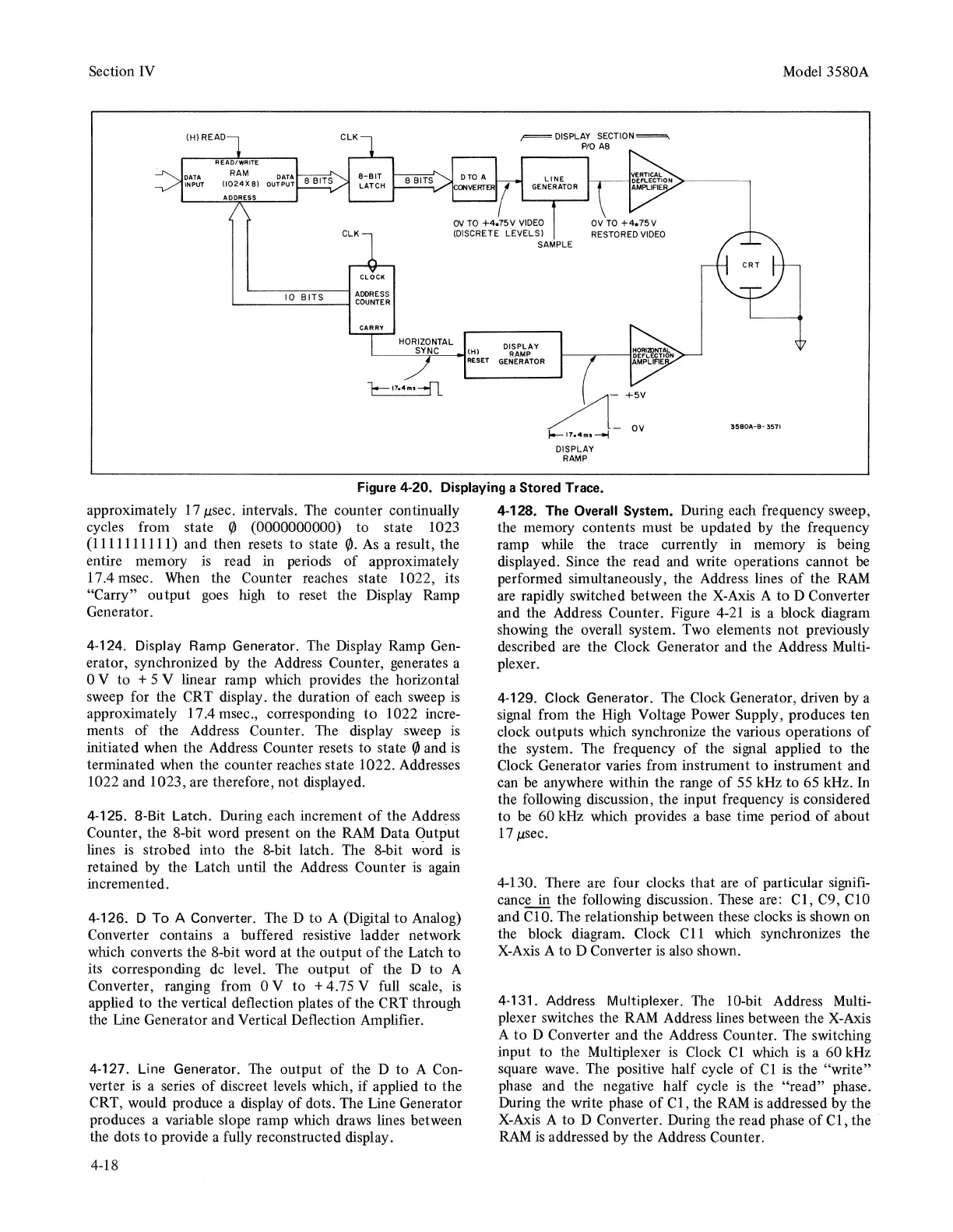
Figure 4-20. Displaying a Stored Trace.
approximately 17
µsec.
intervals. The counter continually 4-128. The
Overall
System. During each frequency sweep,
cycles from state
(/J
(0000000000) to state 1023 the memory contents must
be
updated by the frequency
(1111111111) and then resets
to
state
(/J.
As
a result, the ramp while the trace currently in memory
is
being
entire memory
is
read in periods
of
approximately displayed. Since the read and write operations cannot
be
17.4 msec.
When
the Counter reaches state 1022, its performed simultaneously, the Address lines
of
the
RAM
"Carry" output goes high to reset the Display Ramp
are
rapidly switched between the
X-Axis
A to D Converter
Generator. and the Address Counter. Figure
4-21
is
a block diagram
4-124. Display Ramp Generator. The Display Ramp Gen-
erator, synchronized by the Address Counter, generates a
0 V
to
+ 5 V linear ramp which provides the horizontal
sweep for the CRT display. the duration
of
each sweep
is
approximately 17.4 msec., corresponding
to
1022 incre-
ments
of
the Address Counter. The display sweep
is
initiated when the Address Counter resets to state
(/J
and
is
terminated when the counter reaches state 1022. Addresses
1022 and 1023, are therefore, not displayed.
4-125. 8-Bit Latch. During each increment
of
the Address
Counter, the 8-bit word present on the
RAM
Data Output
lines
is
strobed into the 8-bit latch. The 8-bit word
is
retained by the Latch until the Address Counter
is
again
incremented.
4-126. D To A Converter. The D to A (Digital
to
Analog)
Converter contains a buffered resistive ladder network
which converts the 8-bit word at the output
of
the Latch
to
its corresponding de level. The output
of
the D to A
Converter, ranging from 0 V to + 4.75 V full scale,
is
applied
to
the vertical deflection plates
of
the CRT through
the Line Generator and Vertical Deflection Amplifier.
4-127.
Line
Generator. The output
of
the D to A Con-
verter
is
a series
of
discreet
levels
which,
if
applied to the
CRT, would produce a display
of
dots. The Line Generator
produces a variable slope ramp which draws lines between
the dots
to
provide a fully reconstructed display.
4-18
showing the overall system. Two elements not previously
described
are
the Clock Generator and the Address Multi-
plexer.
4-129. Clock Generator. The Clock Generator, driven by a
signal from the High Voltage Power Supply, produces ten
clock outputs which synchronize the various operations
of
the system. The frequency
of
the signal applied to the
Clock Generator varies from instrument
to
instrument and
can
be
anywhere within the range
of
55
kHz
to
65 kHz.
In
the following discussion, the input frequency
is
considered
to
be
60 kHz which provides a base time period
of
about
17
µsec.
4-130. There are four clocks that
are
of
particular signifi-
cance in the following discussion. These are:
Cl,
C9, ClO
and ClO. The relationship between these clocks
is
shown on
the block diagram. Clock
Cl
l which synchronizes the
X-Axis
A to D Converter
is
also shown.
4-131. Address Multiplexer. The 10-bit Address Multi-
plexer switches the
RAM
Address lines between the
X-Axis
A
to
D Converter and the Address Counter. The switching
input to the Multiplexer
is
Clock Cl which
is
a 60 kHz
square
wave.
The positive half cycle
of
Cl
is
the "write"
phase and the negative half cycle
is
the "read" phase.
During the write phase
of
Cl,
the
RAM
is
addressed
by
the
X-Axis
A to D Converter. During the read phase
of
C 1, the
RAM
is
addressed by the Address Counter.